
Parametric Test and On-Wafer Measurement Teaching Lab
解决方案概述
The Semiconductor Teaching Lab Solution for Parametric Test and On-Wafer Measurement delivers a complete, ready-to-deploy lab that bridges academic instruction with real-world semiconductor engineering practices. This Semiconductor Teaching Lab Solution enables universities to deliver ready-to-teach parametric test and on-wafer measurement labs aligned with real-world semiconductor engineering practices.
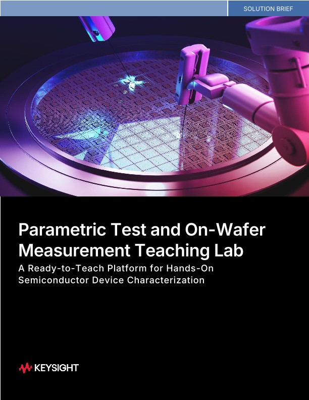
Built around Keysight’s B1500A Semiconductor Device Parameter Analyzer, industry-standard probe stations, and the EasyEXPERT measurement software, this solution enables universities to offer hands-on, structured training in semiconductor device characterization, without the complexity of designing labs from scratch.
The result is a scalable, industry-aligned teaching platform that strengthens workforce readiness and accelerates student learning.