
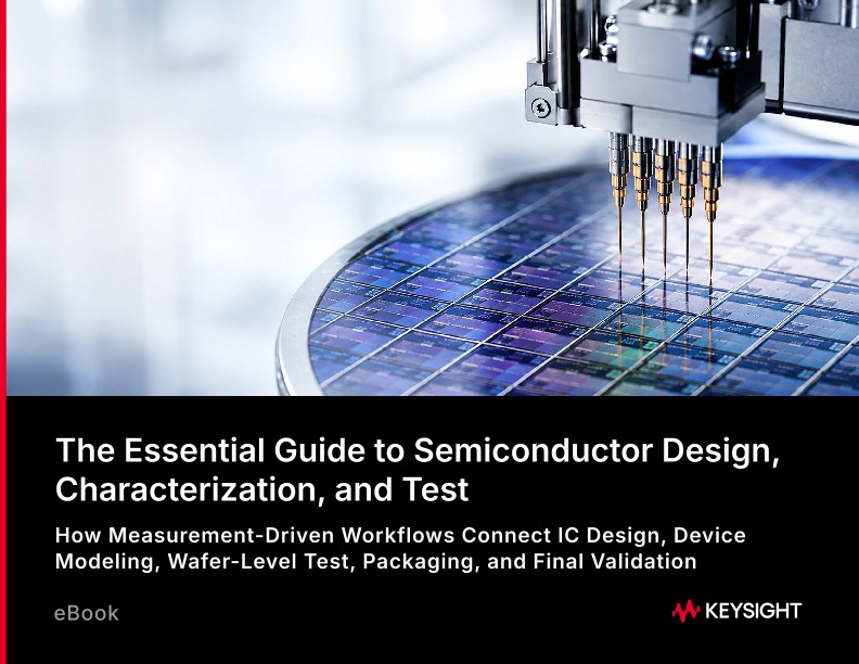
The Essential Guide to Semiconductor Design, Characterization, and Test
eBooks
The Essential Guide to Semiconductor Design, Characterization, and Test explains how measurement-driven workflows connect the semiconductor lifecycle from early IC design through device modeling, wafer-level test, packaging, package test, and final validation. As semiconductor products become more complex, engineering teams can no longer treat design, fabrication, packaging, and test as isolated stages. A design margin decision can affect final test yield. A compact model limitation can hide a corner-case failure until silicon arrives. A small process shift can change leakage, capacitance, resistance, or timing. A package interconnect can introduce parasitics that affect signal integrity, power integrity, RF performance, thermal behavior, and product reliability. This eBook provides a practical end-to-end view of how these stages interact and why connected measurement insight is critical to reducing late-stage risk.
The guide begins by explaining why end-to-end visibility matters in modern semiconductor development. It reframes the traditional linear lifecycle — define the product, design the circuit, fabricate the wafer, package the die, and test the final device — as a feedback system. Measurements from device characterization improve models. Wafer-level test data reveals process behavior. Package test uncovers interconnect and structural risks. Functional validation connects the finished device back to real-world operating conditions. Readers learn how measurement data helps teams improve design confidence, model accuracy, process understanding, yield learning, and product quality.
The eBook then walks through the semiconductor lifecycle at a high level, covering requirements and architecture, design and simulation, device characterization and modeling, mask handoff, wafer fabrication, wafer-level test, packaging, package inspection, and final validation. It explains where measurement fits at each stage and how design intent, physical realization, electrical evidence, and product confidence work together. This lifecycle view helps design engineers, modeling engineers, product engineers, test engineers, validation engineers, packaging teams, and technical managers build a shared understanding of how semiconductor risk moves downstream and how early measurement correlation can reduce the cost of learning.
A major section focuses on IC design and simulation, showing how system-level requirements are translated into measurable electrical targets. It covers RF and microwave IC design, high-speed digital physical-layer design, mixed-signal design, power electronics, MMIC design, electromagnetic effects, and simulation-to-measurement correlation. The guide explains why design verification and test planning should be connected before first silicon and why electromagnetic effects, interconnects, package structures, fixtures, and parasitics must be considered as operating frequencies and edge rates increase.
The device characterization and compact modeling section explains why circuit simulation is only as trustworthy as the models behind it. It covers IV, CV, pulsed IV, S-parameter, noise, and temperature-dependent measurements, along with model extraction, model quality, SPICE model signoff, process design kits, and simulation correlation. Readers learn how compact models turn measured device behavior into simulation-ready representations that support more reliable design decisions.
The eBook also provides wafer fabrication context for test and validation engineers, explaining front-end-of-line, middle-of-line, and back-end-of-line process regions, along with core process modules such as lithography, deposition, etch, ion implantation, annealing, CMP, cleaning, metrology, and inspection. Rather than focusing on fab equipment, the guide emphasizes how physical variation becomes electrical variation and how wafer-level data, wafer maps, distributions, and parametric test results help reveal process signatures.
Additional chapters cover wafer-level and parametric test, power and wide-bandgap semiconductor test, packaging and interconnect validation, and final functional validation. Topics include wafer acceptance test, process control monitoring, leakage, breakdown, threshold voltage, contact resistance, capacitance, known good die, static and dynamic power device characterization, double-pulse testing, SiC and GaN device behavior, package parasitics, wire-bond defects, signal integrity, RF validation, high-speed digital compliance, mixed-signal validation, low-power current profiling, OTA test, MMIC verification, and photonic IC measurement.
The guide concludes with a practical case study that follows a high-speed compliance failure backward through final validation, package effects, wafer-level data, model assumptions, and design margin. The example shows how late-stage failures often result from multiple small margin losses rather than one obvious defect. Overall, this eBook helps semiconductor teams connect point tools into connected insight, enabling better modeling, characterization, wafer-level test, package validation, functional test, and final product confidence.