您希望搜索哪方面的内容?
Keysight EDA Connect World Tour
Join us in a city near you to learn from electronic design automation (EDA) experts, connect with designer communities, and discover how to amplify the value of advanced simulations, leverage AI-driven engineering productivity, and automate open workflows.
30
Cities
21
Technical sessions
1000+
Design professionals
Find the Best Way to Shift Left, Right in Your Backyard
No matter your role — from design engineer to R&D lead — you will find inspirations and tangible solutions to accelerate your design process for high-speed, high-frequency, and high-power products.
See what's possible


Strengthen your expertise in a series of expert-led sessions , customized to your industries and based on real-world case studies.


Get technical training to unlock the power of the newest capabilities inside Keysight EDA solutions.
Find your people


Connect with local and like-minded peers and industry leaders who believe in the transformative power of AI/ML and automation.
Attend expert-led sessions that span a broad range of topics and learn from the most successful design teams in your community.


Module 1: Enable AI-Driven RF Circuit Design
A successful RF design does not just meet the specifications. Explore cutting-edge EDA advancements — from AI-driven design to rapid electromagnetic circuit co-design — to accelerate complex RF circuit design and power a hyperconnected future.

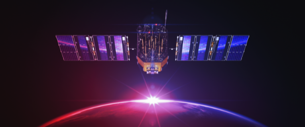
Module 2: Power RF System Design Innovation
Complex system-level design challenges emerge as communications extend into the vastness of space. Explore how Keysight's latest EDA innovations, including integrated RF system/circuit design workflows, RF system modeling, and AI integration for 6G air interface research, are revolutionizing RF system design.


Module 3: Optimize High-Speed Digital Designs
Chiplets are forcing new strategies to cope with more complex thermal, power, and signal integrity issues at the chiplet and package level and multiple die-to-die interfaces. Hear experts' vision on the essential practices to enhance your high-speed digital design workflows to win the chiplet race.


Module 4: Accelerate Photonic Design with Advanced Accuracy
Photonic integrated circuits (PICs) are pervasive, and the accuracy of simulation models is the key factor in achieving reliable PIC designs. Learn about the pivotal role of physics-based models as the foundation for accurate photonic modeling.


Module 5: Streamline Design Data, IP, and Engineering Lifecycle Management
Imagine having all your design data at your fingertips, perfectly organized and easily accessible, empowering you to create innovative designs easily. Discover how a unified data and IP management system can transform your work.

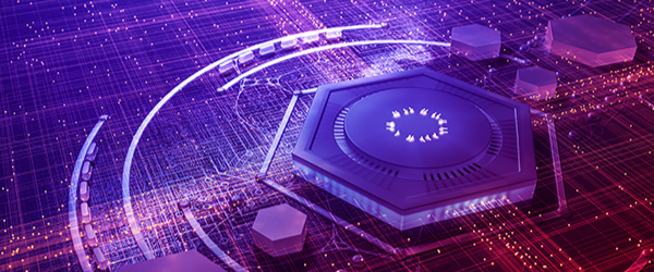
Module 6: Pioneer Quantum Circuit Design
As quantum computing evolves, superconducting qubits have emerged as a promising platform due to their scalability and controllability. Learn how Quantum EDA offers a pathway towards realizing robust and scalable superconducting quantum chips, accelerating progress in quantum computing and quantum information processing.
Find a city near you and register today


Americas
Americas


Europe
Europe


Asia Pacific
Asia Pacific


Greater China
Greater China
Santa Clara - HSD Day | Mar 12
Santa Clara - RF Day | Mar 13
San Diego | Mar 20
Seattle | Apr 8
Vancouver BC | Apr 10
Washington DC | May 14
Denver | Sep 11
Phoenix | Oct 15
Massy - RF Day | Mar 26
Gothenburg - RF Day | Apr 3
Nijmegen - RF Day | Apr 8
Munich - RF Day | May 14
Cardiff - RF Day | May 20
Torino - HSD Day | May 27
Bologna - HSD Day | May 29
Massy - HSD Day | Jul 3
Seoul | May 14
Singapore | May 29
Start Your Next Design with Keysight EDA Tools
The Keysight suite of EDA tools seamlessly integrates device modeling, circuit design, EM simulation, layout capabilities, and system-level modeling. Keysight’s open solutions approach for workflow enablement ensures that our EDA software interoperates with other EDA software from our ecosystem partners. Combine process design kits (PDKs) with our circuit simulators to increase your confidence in achieving design success.
Frequently Asked Questions (FAQs)
Sign up now to be notified if space becomes available or to be the first to know once our Virtual Experience details are released.
All stops are free to attend. You must register for each event you want to attend. If registration is not open for an event you would like to attend, or if you would like to know when we add new cities, please contact us at: [email protected] to receive updates.
Yes. To ensure that attendees receive the most relevant information, the agenda for each seminar is carefully tailored, with papers handpicked by Keysight tech experts. For more details, please check the agenda on the specific registration page.
Please email: [email protected].
Want help or have questions?