What are you looking for?
Design and Simulation of Power Electronics with EDA Tools
In contrast to traditional electronics, which is all about handling data, power electronics is all about handling power: generating it, converting it, and moving it from source to load. This technology finds applications in a wide range of industries including power utility generation and distribution; automotive; and consumer electronics.

Keysight Power Electronics Workflow
Design and simulation using Electronic Design Automation (EDA) tools is the second stage in the workflow that Keysight supports for your power electronics project. The figure and text below explain all four stages:
Power Electronics Workflow

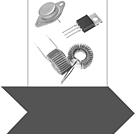
1. Power Device and Component Evaluation
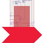
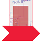
2. EDA for Power Electronics
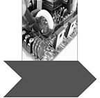

3. Hardware Design and Debug


4. Design Validation/Certification
Keysight’s power electronic workflow consists of four stages:
- Power device and component evaluation. Instruments such as the B1505/6/7 family Power Device Analyzers / Curve Tracers can evaluate devices at very high voltage and current. For more information, see Increasing Reliability and Efficiency in Power Converter Designs Part 1 - Power Device and Component Evaluation.
- The second stage is enabled by EDA tools. Device models can be extracted with our IC-CAP Device Modeling Software and the models added to a complete system simulation (“virtual prototype”) in Advanced Design System (ADS). The design is optimized before committing to a prototype. For more information, see Increasing Reliability and Efficiency in Power Converter Designs Part 2 - EDA for Power Electronics.
- The prototype is measured in stage three, hardware design and debug. For these tasks you can use the power measurement option on a InfiniiVision 3000, 4000, or 6000 X-Series oscilloscope. EMC compliance can be determined by our N6141A/W6141A application for the N9030A/N9020A/N9010A/N9000A Signal Analyzer family, and so on. For more information, see Increasing Reliability and Efficiency in Power Converter Designs Part 3 - Hardware Design and Debug.
- Now that the design is working well, we move to the fourth stage, design validation and certification, where you verify the full functionality of the design through various operating conditions and environments with the PA2200 IntegraVision series of power analyzers and BenchVue software. For more information, see Increasing Reliability and Efficiency in Power Converter Designs Part 4 - Design Validation/Certification.
New Thinking About EDA Tools
The fast dV/dt edges of modern switched-mode converters that benefit from SiC and GaN transistors require new thinking about EDA tools. Traditional SPICE alone is not enough because it is limited to the time-domain and to lumped elements. It does not capture physical layout effects that can dominate performance. In addition, the periodic steady state solution is only produced after a computationally-expensive simulation of the turn-on transient. Frequency-domain techniques like harmonic balance are a more efficient approach to producing the periodic steady state solution.
Keysight EEsof EDA’s products including Advanced Design System (ADS) and Electromagnetic Professional (EMPro) offer both time- and frequency-domain simulation of both lumped and distributed elements. The frequency-domain is covered with our Harmonic Balance (HB) simulator. HB yields the steady state solution rapidly. Distributed effects are covered by our EM field solvers.
There are three main reasons to apply an integrated EM field solver to the “virtual prototype” in your design and simulation workflow:
- The integrated tool flow reduces manual operations, speeds design, and reduces mistakes
- Pinpoint and fix the root cause of, for example, surge voltage overstress from layout parasitics
- Model EMI/EMC in a “virtual chamber”
The simulation yield insights and important performance metrics such as efficiency, and reliability indicators such as surge voltage device overstress.
We have complete platforms for a self-contained workflow for chip, package, and board design and also simulators that plug into Virtuoso from Cadence Design Systems.
Advantages of ADS include:
- #1 EDA tool for high-speed and high-frequency effects at RF, microwave, and above.
- Library of models accurate at hundreds of volts per nanosecond and beyond.
- Accessible and flexible; for example our customizable data display.
- Secure model exchange supply chain via our model encryption technology
For more information go to our simulation hub at https://www.keysight.com/find/eesof-ads
Device Modeling
Keysight is the only vendor that provides your semiconductor component vendors with complete end-to-end modeling solutions. We provide tools for automated measurements, accurate device model extraction, comprehensive qualification, and final process design kit (PDK) validation. As a result, your vendor can provide you the accurate models you need for ADS simulation.
For more information on device modeling go to https://www.keysight.com/find/eesof-device-modeling
Additional Resources
- Power Electronics Resources from Keysight EEsof EDA
- Power Electronics Design with ADS
- Quick Start Guide for ADS in Power Electronics
- W2240BP Power Electronics Bundle: ADS Core, TC, PE Lib, Layout, Momentum