Choose a country or area to see content specific to your location
确认您的国家或地区
中国
请确认
Confirm your country to access relevant pricing, special offers, events, and contact information.
Explore dual-channel and ultra-wideband signal analysis for demanding RF workflows.
Get faster, clearer insights with our new multicore, 12-bit oscilloscope up to 33 GHz. Trade in your old oscilloscope and get credit toward a new XR8.
Bridging design and physical testing to evaluate drop, impact, shock, and vibration compliance before hardware exists.
Unlock your free upgrade to the next bandwidth tier.
Strengthen 1.6T network reliability for AI-scale workloads from transceivers to interconnects.
Pair Keysight VSA software with the new XA5 signal analyzer for advanced visualization, demodulation, and analysis — start your 30-day trial today.
With extra memory and storage, these enhanced NPBs run Keysight's AI security and performance monitoring software and AI stack.
Explore end-to-end workflows spanning IC design, validation, wafer test, and photonics.
Explore curated support plans, prioritized to keep you innovating at speed.
Maximize accuracy and performance with precision accessories engineered for Keysight instruments.
Authoritative application notes, data sheets, reference designs, and test procedures to accelerate design and validation decisions.
Hands‑on bootcamps that teach system design, test methods, and production workflows engineers can apply immediately.
Success Stories
欢迎访问 24x7 自助服务门户网站
其他产品支持
勤学以博览工程师智慧知识宝库
您希望搜索哪方面的内容?
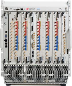
Keysight ParBERT 13.5Gb/s模块是测试各种技术和应用的高速通信端口、元件、芯片和模块等的理想解决方案。
Keysight N4872A 13.5 Gb/s发生器模块和N4873A 13.5 Gb/s分析仪模块均为一个VXI槽宽,并需要E4809A中央时钟模块。ParBERT 13.5 Gb/s模块能产生和分析500 Mb/s 至13.5 Gb/s的差分或单端信号。
ParBERT 13.5 Gb/s模块使Keysight ParBERT 81250最适合下列应用: