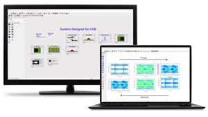
System Designer for USB Video
Product Tours
As USB data rates increase, traditional design workflows are struggling to keep pace. This video highlights how System Designer for USB addresses these challenges—helping engineers reduce time-to-market, catch design issues earlier, and confidently move forward with USB4 designs.
System Designer for USB is a powerful feature in Keysight ADS (Advanced Design System) that accelerates USB4® version 2 design and compliance. Built for high-speed digital design engineers, it enables full end-to-end USB system analysis, from host to device, including interconnects and repeaters—all within a smart, unified environment.
With native support for PAM3 modulation and multi-lane, asymmetric links, System Designer for USB simplifies the setup of complex USB topologies. Engineers can quickly simulate entire systems and perform simulation-driven USB compliance testing using a direct connection to the compliance app. This allows users to validate their designs early in the development cycle and ensure they meet USB4® standards.
The smart components reduce manual setup efforts, cutting 40 mouse clicks down to just 4. The USB Bus Designer enables engineers to define transmission lines and vias before layout, allowing them to predict link performance. Multiple simulation modes enable the analysis of signal integrity metrics within a single schematic.
To support accurate device behavior modeling, the built-in IBIS-AMI model builder generates both Tx and Rx models for NRZ and PAM3 signals. Users can configure equalization settings to ensure realistic performance modeling and faster design convergence.
Watch the video to see how System Designer for USB transforms your USB analysis workflow using Keysight’s advanced simulation and modeling tools.