Choose a country or area to see content specific to your location
您希望搜索哪方面的内容?
-
-
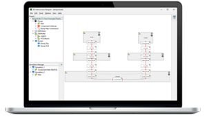
Accelerate Advanced Package & 3DIC Designs
Design, model, and validate complex 3D interconnect architectures with a powerful standalone design environment.

-
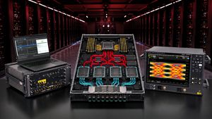
Scale AI Compute. Simplify Validation.
Automate transmitter and receiver validation across next-generation I/O, memory, and fabric interfaces.
-
End-to-End Validation for AI Data Center
Strengthen 1.6T network reliability for AI-scale workloads from transceivers to interconnects.

-
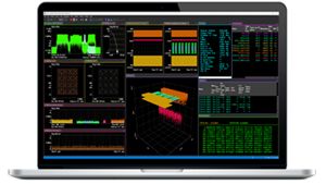
Take On Complex MIMO Signals
Pair Keysight VSA software with the new XA5 signal analyzer for advanced visualization, demodulation, and analysis — start your 30-day trial today.
-
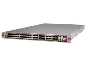
Introducing AI-Enhanced Packet Brokers
With extra memory and storage, these enhanced NPBs run Keysight's AI security and performance monitoring software and AI stack.
-
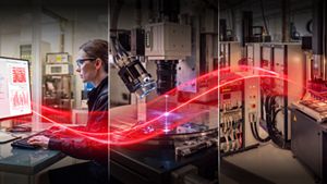
Accelerate Semiconductor Innovation
Explore end-to-end workflows spanning IC design, validation, wafer test, and photonics.
-
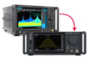
Trade In Before You Buy New
Save up to 50% on our latest instruments with eligible Keysight or competitor trade-ins.
-
-
The Right Connection Makes the Measurement
Maximize accuracy and performance with precision accessories engineered for Keysight instruments.

Trade In Before You Buy NewSave up to 50% on our latest instruments with eligible Keysight or competitor trade-ins.
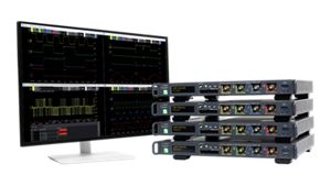
Scale to Hundreds of Channels. Keep Measurements in Sync.Four channels per 1U of rack space, up to 1 GHz bandwidth, and multi-oscilloscope synchronization.
-
-
Purpose-built solutions engineered for the design and test challenges unique to your industry.
Use Cases mapped to every stage of your product lifecycle, from design through operations.
Success Stories
Nokia + Keysight: AI Network Designs at Scale -
Authoritative application notes, data sheets, reference designs, and test procedures to accelerate design and validation decisions.
FeaturedHands‑on bootcamps that teach system design, test methods, and production workflows engineers can apply immediately.
Learning Hub
AI TechnologyExplore methodologies, test strategies, and technical resources for designing, validating, and scaling AI systems and networks.
- 购买
-








All Software Catalog
Explore the complete portfolio of Keysight software, from design engineering tools to emulator and instrument software, built to extend and enhance your Keysight instruments. Whether you are configuring measurements, automating tests, analyzing data, or validating compliance, use the filters below to identify the right software to support your workflow — from design and validation through manufacturing and deployment.

Showing 3 of 3
No Filter available
No Filter available
No Filter available


用于先进建模的功率器件测量系统
通过您可以信赖的仿真建立真实功率器件模型,缩短设计周期。
通过您可以信赖的仿真建立真实功率器件模型,缩短设计周期。
用于先进建模的功率器件测量系统
PD1000A
通过您可以信赖的仿真建立真实功率器件模型,缩短设计周期。
- 轻松创建您可以信赖的仿真模型,从而在您的工作台上就能对任何宽带隙半导体器件进行真实测量
- 控制软件使您可以简便地访问先进测量功能,以便从这些系统收集建模参数:曲线追踪仪、s 参数和双脉冲测试仪
- 曲线追踪仪系统测量 I-V 和 C-V 特征(静态特征)
- S 参数系统测量接通和关断状态下的 S 参数(寄生特征)
- 双脉冲测试仪可以完成各种模型表征和参数提取任务,例如提取开关、反向恢复、栅极电荷、开关自动定位(switching locus)以及许多其他参数(动态特征)
- W8598BP 电力电子模型生成器软件输入收集到的测量结果,以创建先进的功率器件模型
- 在是德科技 ADS、EMPro 和 Momentum 环境中,可以使用模型执行精准的仿真
混动汽车和电动汽车(HEV/EV)市场正在飞速发展。市面上的车辆电气化程度不断提高,给汽车设计和制造带来了新的挑战。许多 HEV 和 EV 制造商开始使用碳化硅(SiC)和氮化镓(GaN)等宽带隙(WBG)器件进行功率转换设计,以便在更小、更轻和温度更低(散热更少)的封装内实现更高的效率(扩展的范围)和更大的功率。不过,要确保这些新设计安全可靠,需要考虑许多重要问题。
是德科技与 HEV/EV 功率转换市场中的行业领导者紧密合作,帮助他们顺利完成过渡,在其设计中使用WBG 器件。利用这些关系,是德科技开发出了功能十分强大的建模套件和功率电路仿真器工具,使 WBG 器件设计人员能够比以往更轻松地创建模型。测试套件(其中包括曲线追踪、S 参数和双脉冲测试仪硬件)根据真实 WBG 器件进行测量,并使用先进的建模软件来构建是德科技独有的复杂 WBG 器件模型。随后,是德科技先进设计系统软件可以使用这些模型仿真和分析高频分量对设计可靠性和 EMI 的影响。在进入原型设计阶段之前,工程师就可以对设计进行修改,避免不必要的设计过程,从而节省时间和成本。

PathWave PEPro
专门用于设计电源转换器,适用行业包括发电/输电、航空航天与国防、汽车、数据中心、消费电子以及物联网等。
专门用于设计电源转换器,适用行业包括发电/输电、航空航天与国防、汽车、数据中心、消费电子以及物联网等。
PathWave PEPro
W3035E
专门用于设计电源转换器,适用行业包括发电/输电、航空航天与国防、汽车、数据中心、消费电子以及物联网等。
W3035E PathWave PEPro 组件包括以下功能特性:
- 快速开发更完整的高电压、大电流电力电子设计,并且将电路板版图寄生效应考虑在内
- 综合设计技术结合专为基于版图的设计提供的先进技术,让您能够在开始设计硬件原型之前捕获由寄生效应引发的错误
是德科技的电力电子解决方案包括电磁求解器等分析功能,能够仿真版图寄生效应对电路板的影响。 内层近场可视化是电力电子专业版(PEPro)设计软件套件中的一项新功能,它对于您查看电流和场、实现长期可靠性至关重要。 您可以探索各方面的电流收缩,这个特性可能会产生热效应并影响可靠性。 电路板分析功能支持矩量法(MoM)平面仿真,以及使用有限元法(FEM)分析 3D 效应。
注:这个组件许可证需要配合主机套件才能正常使用。 如需了解建议的套件配置,请点击 此处。


PathWave ADS Core + EM Design + Layout + PEPro + PE Ckt Sim
W3631B is designed for power converter design for power generation and transmission, AD, automotive, data center, consumer electronics, and IoT applications.
W3631B is designed for power converter design for power generation and transmission, AD, automotive, data center, consumer electronics, and IoT applications.
PathWave ADS Core + EM Design + Layout + PEPro + PE Ckt Sim
W3631B
W3631B is designed for power converter design for power generation and transmission, AD, automotive, data center, consumer electronics, and IoT applications.
The W3631B PathWave ADS Core + EM Design + Layout + PEPro + PE Ckt Sim includes:
- Quickly design the most complete high-voltage and high-current power electronic designs including the effects of board layout parasitics
- Integrated design technology with advanced technologies for layout-based design engineered to capture parasitically induced faults before hardware prototyping
- Prebuild test benches that quickly reports simulated EMI and EMC compliance to international standards
Keysight’s solution for power electronics includes both device modeling and power electronics simulation, and includes Power Electronics Pro (PEPro) analysis capabilities such as harmonic balance for precise analysis of periodic steady state signals and closed loop analysis. It also includes transient design simulation for analysis of the switching characteristics including the open loop analysis. The electromagnetic (EM) solver enables the simulation of board effects from layout parasitics. New in the PEPro design suite is an inner layer near-field visualization, very important to look at the currents and fields for long-term reliability. You can discover areas of current constriction, which may cause heating effects and affect reliability. The analysis of the boards supports both the method of moments (MoM) planar simulation, as well as a finite element method (FEM) for 3D effects.
