Choose a country or area to see content specific to your location
确认您的国家或地区
请确认
Confirm your country to access relevant pricing, special offers, events, and contact information.
Explore dual-channel and ultra-wideband signal analysis for demanding RF workflows.
Get faster, clearer insights with our new multicore, 12-bit oscilloscope up to 33 GHz. Trade in your old oscilloscope and get credit toward a new XR8.
Bridging design and physical testing to evaluate drop, impact, shock, and vibration compliance before hardware exists.
Unlock your free upgrade to the next bandwidth tier.
Strengthen 1.6T network reliability for AI-scale workloads from transceivers to interconnects.
Pair Keysight VSA software with the new XA5 signal analyzer for advanced visualization, demodulation, and analysis — start your 30-day trial today.
With extra memory and storage, these enhanced NPBs run Keysight's AI security and performance monitoring software and AI stack.
Explore end-to-end workflows spanning IC design, validation, wafer test, and photonics.
Explore curated support plans, prioritized to keep you innovating at speed.
Maximize accuracy and performance with precision accessories engineered for Keysight instruments.
Purpose-built solutions engineered for the design and test challenges unique to your industry.
Use Cases mapped to every stage of your product lifecycle, from design through operations.
Success Stories
Authoritative application notes, data sheets, reference designs, and test procedures to accelerate design and validation decisions.
Hands‑on bootcamps that teach system design, test methods, and production workflows engineers can apply immediately.
Learning Hub
Explore methodologies, test strategies, and technical resources for designing, validating, and scaling AI systems and networks.
欢迎访问 24x7 自助服务门户网站
其他产品支持
勤学以博览工程师智慧知识宝库
您希望搜索哪方面的内容?
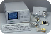
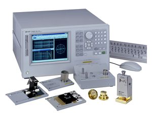
Keysight 4291B射频阻抗/材料分析仪是针对表面封装元器件和介电/磁性材料的高精度测量的完整解决方案。与反射测量技术不同,Keysight 4291B使用直接的电流-电压测量技术,可在广泛的阻抗范围内提供更精确的阻抗测量结果。
基本阻抗精度是+/- 0.8%。高Q精度有利于进行低损耗元器件分析。内置合成器扫频范围从1 MHz到1.8 GHz,具有1 MHz的分辨率。1.8米长的精密电缆可将分析仪连接到测试站,以便您将测试点延伸到分析仪之外,而不会影响测量精度。先进的矩阵和错误补偿功能消除了夹具的测量错误,确保DUT/MUT的高精度和可重复性。
Keysight 4291B还提供自动电平精度控制和用IBASIC程序功能监视测试信号;可在恒压或恒流下测量器件。用可选的直流偏置(达40V和100mA)使测量偏置独立于阻抗特性。只要按一个按钮,内装的等效电路分析功能就自动计算5种电路模型的电路常数值。
Keysight 4291B有2个测量通道;每一个通道都可设置为测量1个(即Z)或2个(即Z-theta)阻抗参数。具有分割显示的彩色TFT可显示有效示踪和存储器示踪(保存在RAM中)。内部软盘驱动器以LIF或MS-DOS格式保存程序和测试数据。有了内装IBASIC,您就能从Keysight 4291B直接控制恒温箱或园片探测器这类外部测试设备,而不需要单独的仪器控制器。
材料评估
Keysight 4291B能容易地进行全面的材料评估,提高材料评估的质量和效率。Keysight 4291B提供宽频率范围(1MHz至1GHz)介电/磁性材料测量的总体解决方案。