这是您想要的页面.
查看搜索结果:
您希望搜索哪方面的内容?
建议的搜索
No product matches found - System Exception
符合的结果


- 概述和特性
- 售后升级
- 资源
HIGHLIGHTS
先进设计系统(ADS)先进版图组件:
- 版图与原理图(LVS)
- 设计规则检查(DRC)
- 第三方 DRC 和 LVS 工具
- 制造网格
- 硅基虚拟金属填充实用程序
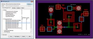
 先进设计系统(ADS)W2320EP 先进版图组件允许您使用其他 ADS 版图功能进行版图验证,另外还允许您使用制造网格和硅基射频集成电路实用程序。
版图与原理图(LVS)
- ADS 模块 LVS
- LVS 可用于多技术模块设计
- 模块设计包含带有区域引脚的集成电路封装或带有焊盘元器件的嵌套集成电路
- 检查模块级连接以及通过键合线到集成电路中焊盘的连接。(技术创新申请中)
- ADS 器件识别 LVS
基于规则的 LVS,用于集成电路设计
- ADS 物理 LVS
用于集成电路和射频电路板设计的 LVS,以版图中的物理连接为基础
使用元器件区域引脚和层绑定来形成物理网络。包括形成物理网络时导电层上的各种形状,从而提供准确的短路检测。(已获技术创新)
- ADS 引脚网络 LVS
能够轻松诊断 LVS 错误
运行 引脚网络 LVS 来检查每个子设计是否达到 LVS 洁净标准
使用分层视图浏览设计,并检查每一层的映射元器件
- 来自原理图中的版图网络名称
使用“与原理图的差异”对接窗口将原理图中的网络名称引入版图
版图网络名称会出现在 Navigator 和 LVS 报告中,方便识别和突出显示重要的网络
设计规则检查(DRC)
用于集成电路、模块和射频电路板设计的 DRC
选择规则类别以便运行一部分规则,或运行全套规则并在后台进行 DRC,同时版图窗口仍保持激活状态
ADS DRC 在本地计算机上运行,确保数据安全
DRC 和 LVS 第三方工具
- 在版图窗口中运行 DRC 和 LVS 第三方工具并突出显示错误
- 将第三方 DRC 结果导入 DRC 对话框
制造网格
- 识别不在网格中的版图对象,并通过手动网格外覆盖将网格对象与制造网格快速对齐
硅基射频集成电路实用程序
- 为硅基射频集成电路生成虚拟金属填充
- 检查设计是否符合目标要求的金属密度
- 在设计过程的早期使用 Momentum 验证设计的金属填充效果
排序依据 :
日期
日期
标题
Filter Results
没有找到与该产品有关的信息。
重置
按内容类型