这是您想要的页面.
查看搜索结果:
您希望搜索哪方面的内容?
建议的搜索
No product matches found - System Exception
符合的结果

- 概述和特性
- 售后升级
- 资源
HIGHLIGHTS
SIPro 的主要优势包括:
- 出色的分析速度和精度 ― 与速度很快但精度受到限制的混合型电路电磁分析工具不同,SIPro 建立在纯粹的电磁技术之上,提供接近业界标准三维电磁求解程序的分析精度。SIPro 中的电磁技术针对信号完整性(SI)应用进行了专门调试,分析速度和效率远远超过通用的电磁分析工具。
- 易用性设计 ― SIPro 采用与先进设计系统(ADS)一样的通用图形用户界面(GUI),并且该界面针对 SI 分析进行了专门设计。使用网络驱动的使用模式,快速和简单地导航和设置对复杂 PCB 的电磁仿真。借助 SIPro 中的大容量求解程序,您再也不用像使用通用电磁分析工具那样,花费好几个小时手动简化设计,例如 cookie 剪切(cookie-cutting)、删除层和网络。另外,设置电磁端口和求解程序的自动化程度也远高于通用电磁分析工具。
- 紧密结合的工作流程 ― 应用一个同时支持 SI 和 PI 分析的通用环境,您可以在不同分析类型之间轻松复制设置。由此获得的电磁模型可以无缝传送回原理图,使用瞬态仿真器和通道仿真器进行进一步仿真。该流程可以避免在不同点工具之间进行切换,从而节省了宝贵的设计时间。
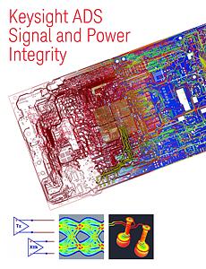 SIPro 提供对高速 PCB 的信号完整性(SI)分析,使您能够表征信号网的损耗和耦合,最终提取出可以在 ADS 瞬态和通道仿真器中使用的精准电磁模型。
SIPro 工作流程
SIPro 的工作流程包括设计导入、分析设置、仿真以及旨在进行更深入仿真的自动原理图生成等环节。
设计导入
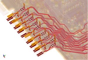
PCB 版图设计可以使用 ODB++、.brd(Cadence Allegro)和 ADFI 格式导入到 ADS 中。导入之后,设计在 SIPro / PIPro 分析环境中打开。您可以在此环境中查看、缩放和三维旋转该设计。
SIPro 分析设置
选择分析中包括的网络和元器件。定义每个网络的 I/O 端口。指定分析的频率范围。

图 1. 网络驱动的使用模式和流程。
SIPro 仿真
您可以在 SIPro 中执行以下分析:
电磁模型提取
- 生成精准的电磁模型,以捕获信号网络损耗和耦合
- 频域 s 参数结果
- 时域 TDR 结果

图 2. 容易地绘制单端、差分、混合模式仿真结果,以查看传输串扰、TDR 等参数。
完整的通道分析
- 提取出的电磁模型可以再送回原理图,然后在 ADS 瞬态和通道仿真中直接使用
SIPro 和 PIPro 产品配置
| W2223BP/BT ADS 捆绑套件 |
W2224BP/BT ADS 捆绑套件 |
W2359EP/ET PIPro 元件* |
W2360EP/ET SIPro 元件* |
|
|---|---|---|---|---|
| ADS Core 环境 |  |
|
||
| ADS 版图 | |
|
||
| 瞬态卷积仿真 | |
|
||
| 通道仿真 | |
|
||
| 可控阻抗线路设计软件 | |
|
||
| Momentum 电磁分析 | |
|||
| PIPro 电磁分析 | |
|
|
|
| SIPro 电磁分析 | |
|
|
* SIPro 和 PIPro 元件需要与 ADS Core 环境和 ADS 版图一起使用。
排序依据 :
日期
日期
标题
Filter Results
没有找到与该产品有关的信息。
重置
按内容类型