
How to Simulate Low Voltage, High Power 2000 Amps to a Dynamic Digital Load
Article Reprints
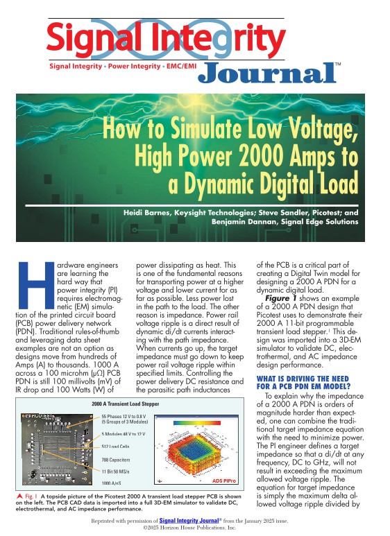
Including the EM behavioral model of the PCB PDN parasitics is now a critical part of designing and validating a 2000 A PDN. The orders of magnitude drop in ZTarget from hundreds of mohms to tens of μohms is driving the need for higher fidelity PI PDN Digital Twin simulations that include a dynamic switching VRM model, the PCB PDN EM model, and a worst-case transient load model to validate the design before fabrication. Behavioral VRM models like the Sandler SSAM and transient load switch models that run in HB have a significant simulation time savings advantage by jumping directly to the steady state results for fast optimization and debugging of a design. Digital Twin HB simulations can run in a matter of seconds or minutes compared to transient simulations, which can take hours or even days when including the PCB EM model. Creating the PCB PDN EM model also continues to get easier. EM simulators that are optimized for PCB PDN simulations provide an increased level of automation to enable the basics of DC IR Drop, electrothermal, and AC impedance for early detection of design issues. The ability to optimize a PDN for Z Target with PCB parasitics in the frequency domain and to then export to an end-to-end PI Digital Twin simulation for validation in the time domain should be standard practice for the PI engineer.