
Scaling AI Infrastructure from Chip to Cluster
Posters
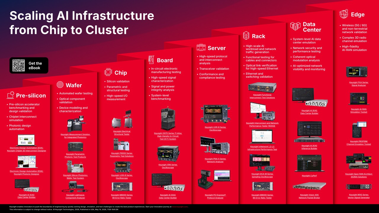
Scaling AI Data Centers frames AI infrastructure as an end-to-end system whose limits emerge when components are pushed together at scale. It opens by noting that AI-scale computing pushes every layer of the data center, and that improving one layer often shifts performance pressure to another. From this starting point, the document presents Keysight’s chip-to-cluster view of the AI infrastructure ecosystem, spanning pre-silicon work through wafer, chip, board, server, rack, data center, and edge.
At the pre-silicon layer, the message is that scaling problems begin with design choices. Multi-die architectures and integrated photonics require engineers to model system behavior before hardware exists. The document highlights early benchmarking and design validation by emulating AI-scale workloads inside design workflows, along with chiplet interconnect simulation that uses silicon measurement feedback to improve correlation, and photonic design automation to streamline photonic integrated circuit design.
The wafer layer focuses on where AI-specific physical limits first appear. High-density optical interfaces and aggressive I/O bandwidth push thermal, electrical, and photonic boundaries. The guide emphasizes automated silicon and silicon photonics wafer test with high-speed electrical and optical characterization, optical component validation, and device modeling for technologies such as silicon and gallium nitride, with the goal of defining margins before weak points become downstream failures.
The chip layer bridges wafer foundations into GPUs, memory, and other subsystems that must operate inside AI compute fabrics. Keysight support is described for post-silicon validation of die-to-die interconnect standards such as UCIe, especially as bandwidth and signal integrity limits tighten and pre-silicon models cannot fully predict real-world behavior. It also highlights high-throughput parametric and electrical structural testing, advanced packaging related measurements, and high-speed I/O measurement for elements such as SerDes, clocking, and retimers.
At the board or PCB layer, the emphasis is whether silicon performance holds up in the physical world. AI-driven requirements stress PCBs with higher frequencies, greater crosstalk risk, and tighter latency margins. The document lists in-circuit manufacturing test to detect parasitic effects and stray coupling, transmitter and receiver characterization for PCIe, CXL, DDR, and HBM, and debugging for signal integrity, power integrity, and electromagnetic interference. It also points to system-level benchmarking to emulate many boards and AI workloads so teams can validate post-silicon designs and I/O channels at system scale.
The server layer describes AI servers as tightly orchestrated compute ecosystems, with GPUs, CPUs, DPUs, memory, optical engines, and network fabrics that must behave as a synchronized whole. It covers protocol and interconnect analysis, transceiver validation for 800G and 1.6T Ethernet, power, timing, and thermal characterization, and conformance and compliance testing to support current and next-generation standards.
At the rack layer, stacking servers changes the governing performance variables. Latency, flow control, and collective operations become dominant, and a single misbehaving node or link can stall thousands of GPUs. The guide highlights high-scale AI workload and network traffic generation that replicates training and inference patterns, electrical and optical link verification across cables, connectors, and transceivers, and Ethernet and switching validation for AI transports such as RoCEv2 and Ultra Ethernet.
At full data center scale, challenges expand into power distribution, thermal constraints, fiber reliability, optical transport, and multi-data center synchronization. The document describes security and performance testing tailored to AI-native data flows, system-level AI data center emulation to validate clusters before deployment, coherent optical modulation analysis for multi-terabit backbone links, and AI-optimized network visibility and monitoring for usage and security insights.
Finally, the edge section explains that when inference moves outward, performance becomes a network engineering problem driven by latency, mobility, spectrum conditions, and core capacity. It highlights wireless validation for 5G, 6G, and non-terrestrial networks, complex 3D channel emulation, and AI-RAN simulation that produces high-scale models and datasets for training, testing, and benchmarking.
The close ties the narrative together: the AI ecosystem advances by solving constraints one layer at a time, but each solution pushes pressure onto the next. For that reason, multi-layer challenges require multi-level expertise, combining deep physics-based insight at each layer with the system-level capability to connect them.