Choose a country or area to see content specific to your location
确认您的国家或地区
中国
请确认
Confirm your country to access relevant pricing, special offers, events, and contact information.
Pinpoint interference with post-processing spectrum management software in the lab.
Use this selector tool to quickly identify the best power supply for your aerospace and defense ATE requirements.
3D Interconnect Designer provides a flexible modeling and optimization environment for any advanced interconnect structure, including chiplets, stacked die, packages, and PCBs.
Get faster digital validation for less with a trade-in.
Emulate every part of your data center infrastructure. Emulate Anything. Optimize Everything.
With extra memory and storage, these enhanced NPBs run Keysight's AI security and performance monitoring software and AI stack.
Achieve fast, accurate board-level testing with robust inline and offline ICT designed for modern manufacturing.
Explore curated support plans, prioritized to keep you innovating at speed.
Authoritative application notes, data sheets, reference designs, and test procedures to accelerate design and validation decisions.
Hands‑on bootcamps that teach system design, test methods, and production workflows engineers can apply immediately.
Success Stories
欢迎访问 24x7 自助服务门户网站
其他产品支持
勤学以博览工程师智慧知识宝库
您希望搜索哪方面的内容?
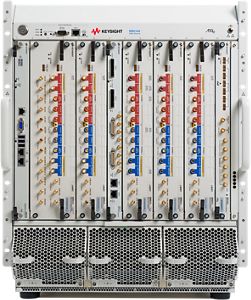
Electrical modules:
Keysight ParBERT 81250 3.35Gb/s模块使ParBERT 81250成为测试10 Gigabit Ethernet 、XAUI器件,以及用于一些串行总线(S-ATA, Firewire, PCI-Express,.)和背板半导体产品高速通信端口的理想设备。
有了3.35Gb/s ParBERT模块,就能在64个通道上测试并行和多串行从21Mb/s直至3.35Gb/s的速度。E4861B为一个VXI槽宽,可包含2种前端插卡(E4862B: 3.35 Gb/s 发生器前端或E4863B: 3.35 Gb/s 分析仪前端)。
串行总线 (S-ATA, Firewire, PCI-Express, Infiniband,..) 和背板应用 3.35Gb/s前端优异的抖动性能和脉冲保真度使其成为设计、评测和在研发及制造中验证高速通信端口、元件、芯片及模块的理想设备。
更多信息: