Choose a country or area to see content specific to your location
您希望搜索哪方面的内容?
Design, model, and validate complex 3D interconnect architectures with a powerful standalone design environment.
Automate transmitter and receiver validation across next-generation I/O, memory, and fabric interfaces.
Strengthen 1.6T network reliability for AI-scale workloads from transceivers to interconnects.

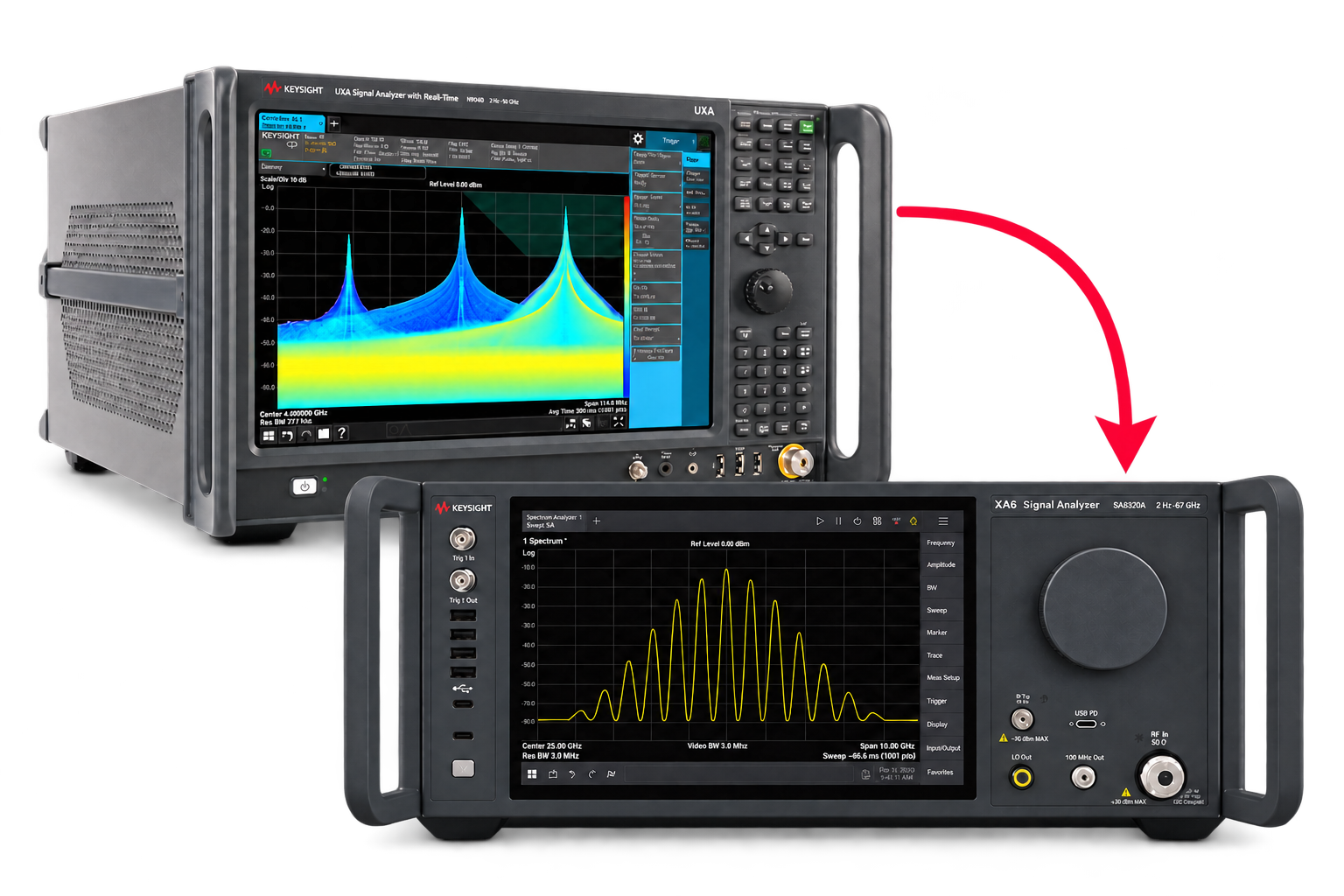
Pair Keysight VSA software with the new XA5 signal analyzer for advanced visualization, demodulation, and analysis — start your 30-day trial today.
With extra memory and storage, these enhanced NPBs run Keysight's AI security and performance monitoring software and AI stack.
Explore end-to-end workflows spanning IC design, validation, wafer test, and photonics.

Save up to 50% on our latest instruments with eligible Keysight or competitor trade-ins.
Maximize accuracy and performance with precision accessories engineered for Keysight instruments.
Save up to 50% on our latest instruments with eligible Keysight or competitor trade-ins.
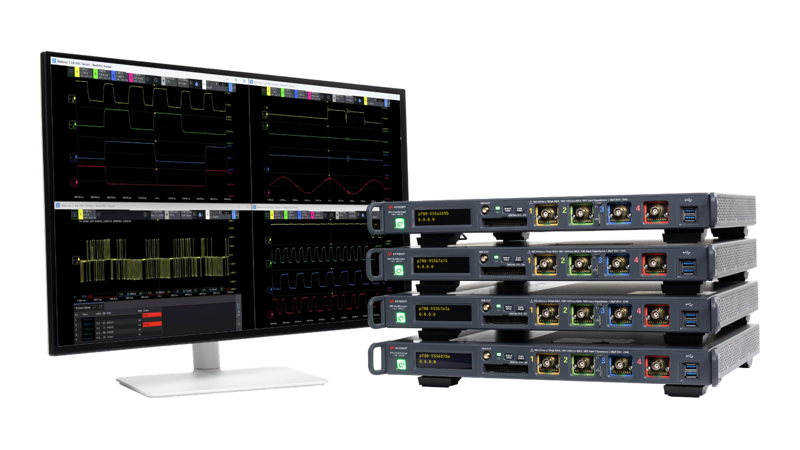
Four channels per 1U of rack space, up to 1 GHz bandwidth, and multi-oscilloscope synchronization.
Purpose-built solutions engineered for the design and test challenges unique to your industry.
Use Cases mapped to every stage of your product lifecycle, from design through operations.
Success Stories
Authoritative application notes, data sheets, reference designs, and test procedures to accelerate design and validation decisions.
Hands‑on bootcamps that teach system design, test methods, and production workflows engineers can apply immediately.
Learning Hub
Explore methodologies, test strategies, and technical resources for designing, validating, and scaling AI systems and networks.
Discover the next generation of electronic design automation software.
Predict and optimize designs before tape-out and fabrication.
In today’s race to deliver breakthrough innovations, success is determined by innovative design before the first prototype is built. Engineers must account for increasing interactions across devices, circuits, systems and physical implementation for electromagnetic, electrothermal, and multi-physics effects, so that every design decision moves them closer to first-pass success. Keysight EDA software brings these critical workflows together in an open, AI-assisted environment that spans device modeling, RF circuit-electromagnetic-electrothermal-system design simulation and optimization, 3D physical layout, multi-physics analysis, and traceable data management.
By combining industry-leading simulation accuracy, measurement-driven insights, validated foundry process design kits (PDKs), Agentic AI tools and processes into an open interoperable ecosystem, and Keysight helps engineering teams reduce risk, accelerate design throughputs, and transform bold ideas into market-ready products with greater speed and certainty.
Turnkey solutions for device modeling and characterizing CMOS, RF, and III-V devices.
RTL power analysis and optimization platform to model, debug, and reduce chip power.
The automated way to reduce the time and resources used during design verification across simulation and test.
RF teams evaluate only a fraction of the available design options, as complex electromagnetic simulations can take days or weeks. Decisions are made on partial information, and problems are only found at fabrication, where they are expensive to correct. Learn how to leverage agentic AI in ADS, enabling you to set the performance a circuit needs to meet, and have AI agents then carry out the design work without scripting.
Explore this range of EDA Bootcamps for e-learning on specific design topics. Combining webinars, videos, application notes, case studies and blogs, this is a bookmark that you will want to share.
Keysight EDA offers a Startup Program for qualifying companies to help you be successful. Keysight provides aggressive discounts for Keysight EDA products to help maintain a healthy cash flow. Keysight will promote your early success to build investor credibility, attract additional funding, and promote potential acquisition.
Electronic design automation (EDA) is a Computer-Aided Design (CAD) category of software tools for designing electronic circuits and systems. The tools work together in a specific design flow for the physical design of chips, packages, and boards.
EDA software can perform individual device characterization, and the electrical design of the interconnects between active electronics from the component to the system level.
Keysight’s EDA software includes tools for circuit design, physical design, system design, device modeling, signal and power integrity, interconnect design, and data and IP management. Some of the key tools are Advanced Design System (ADS), RFPro, SIPro, PIPro, Chiplet PHY Designer, GoldenGate, and SystemVue.
Virtual prototyping involves building a soft equivalent of a design before investing in hardware prototyping. Statistical studies examine how a design behaves under many operating conditions. Product variations could include high volume or temperature, voltages, and signal environments. Yield analysis examines building the design in single quantities or mass production.
The principal simulation is circuit simulation, which can be performed in both time and frequency domains. A range of additional tools can help optimize a design. Statistical analyses perform optimization and parameter sweeps to improve aspects of a circuit. Electrothermal analysis relates heat impacts to a circuit's electrical characteristics. Electromagnetic analysis describes the electromagnetic effects on a circuit's electrical characteristics.
EDA software enables design confidence by analyzing design performance, catching errors before build-out, and helping to avoid the cost of board respins. EDA software improves and perfects the design performance, reducing the cost of physical materials and improving manufacturability and yield. Described as a Shift Left approach, leveraging EDA software earlier in the design cycle reduces overall design engineering time.
Keysight EDA software improves design accuracy through advanced simulation technologies, including RFIC, EM, and electro-thermal analysis. These technologies, combined with integrated design guidance for the latest high-speed digital standards (UCIeTM, PCIe® 6, USB4v2, and DDR5), provide precise simulations that help validate designs early in the design process.
Ever-increasing substrate layer counts, smaller form factors, complex packaging technologies, and closer design proximities continue to make designs ever more challenging. Keysight ADS is the industry-proven multi-technology 3D layout and integrated EM-circuit co-simulation platform for designing RF modules that contain RFICs, packaging, antennas, and RF Printed Circuit Boards (PCBs).
Keysight infuses our robust, accurate, easy-to-use design and validation solutions with advanced simulation techniques and critical measurement science know-how from over 80 years of test industry experience. For example, shared technology between simulation and test eliminates discrepancies and delays when matching results from complex multi-technology RF modules for 5G, automotive radar, and aerospace applications.
Keysight provides specialized tools like ADS and RFPro, which are tailored for high-speed digital and RF design. These tools offer accurate modeling, simulation, and optimization capabilities essential for designing complex RF and high-speed digital systems.
Talk to our team to find the right solution for your design needs, get a personalized quote, or request a free trial.
您希望搜索哪方面的内容?