Choose a country or area to see content specific to your location
您希望搜索哪方面的内容?
Design, model, and validate complex 3D interconnect architectures with a powerful standalone design environment.
Automate transmitter and receiver validation across next-generation I/O, memory, and fabric interfaces.
Strengthen 1.6T network reliability for AI-scale workloads from transceivers to interconnects.

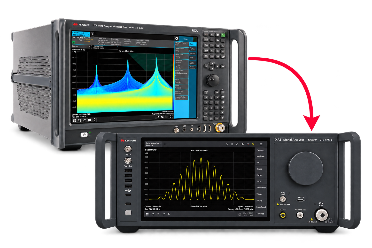
Pair Keysight VSA software with the new XA5 signal analyzer for advanced visualization, demodulation, and analysis — start your 30-day trial today.
With extra memory and storage, these enhanced NPBs run Keysight's AI security and performance monitoring software and AI stack.
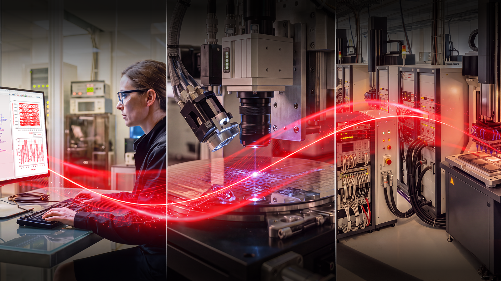
Explore end-to-end workflows spanning IC design, validation, wafer test, and photonics.

Save up to 50% on our latest instruments with eligible Keysight or competitor trade-ins.
Maximize accuracy and performance with precision accessories engineered for Keysight instruments.
Save up to 50% on our latest instruments with eligible Keysight or competitor trade-ins.
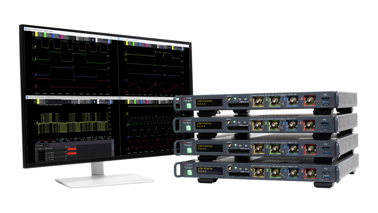
Four channels per 1U of rack space, up to 1 GHz bandwidth, and multi-oscilloscope synchronization.
Purpose-built solutions engineered for the design and test challenges unique to your industry.
Use Cases mapped to every stage of your product lifecycle, from design through operations.
Success Stories
Authoritative application notes, data sheets, reference designs, and test procedures to accelerate design and validation decisions.
Hands‑on bootcamps that teach system design, test methods, and production workflows engineers can apply immediately.
Learning Hub
Explore methodologies, test strategies, and technical resources for designing, validating, and scaling AI systems and networks.
Faster design cycles of superconducting chips.
Accelerate quantum hardware design—from layout to system analysis.
Layout • EM • Circuits • Systems
Keysight Quantum Design Suite connects layout, electromagnetic, circuit, and quantum-system simulation in an integrated workflow. Engineers can create simulation-ready layouts, extract quantum parameters, analyze nonlinear circuit behavior, and evaluate control sequences and cryogenic effects before fabrication—supporting earlier design decisions and fewer physical iterations.
EDA platform for Quantum Design Suite.
Keysight ADS is the premier electronic design automation (EDA) platform for the design of physical layer components that enables engineers to design, analyze, and optimize the critical components that power today's most advanced commercial and defense systems. The base platform contains powerful 3D physical layout and verification, data display, optimization, statistical analysis, Python scripting automation, and AI-Assisted design tools. High-Performance Computing (HPC) options can significantly accelerate simulation times. Additional simulation capabilities such as nonlinear circuit, electromagnetic (EM), electrothermal (ETH) and system provide engineering teams with a choice of value-packed, preconfigured combinations of software modules built for specific design workflows: RF/Microwave, High-speed Digital, Power Electronics, Photonic, and Quantum.
Quantum System Design provides a design environment that accelerates the development of complex quantum systems.
Quantum Circuit Simulation offers a comprehensive circuit design environment that accelerates the development of complex quantum circuits.
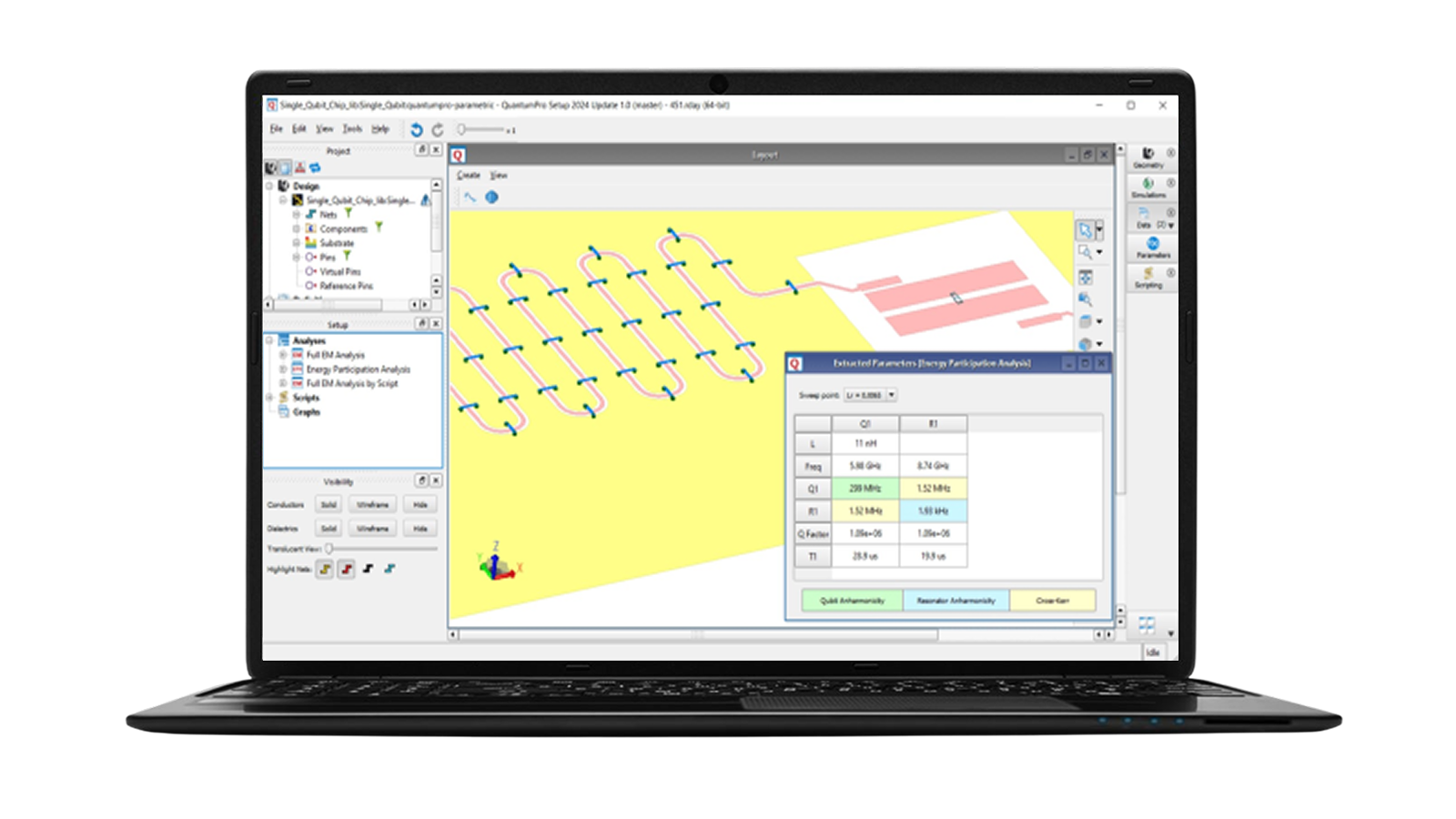
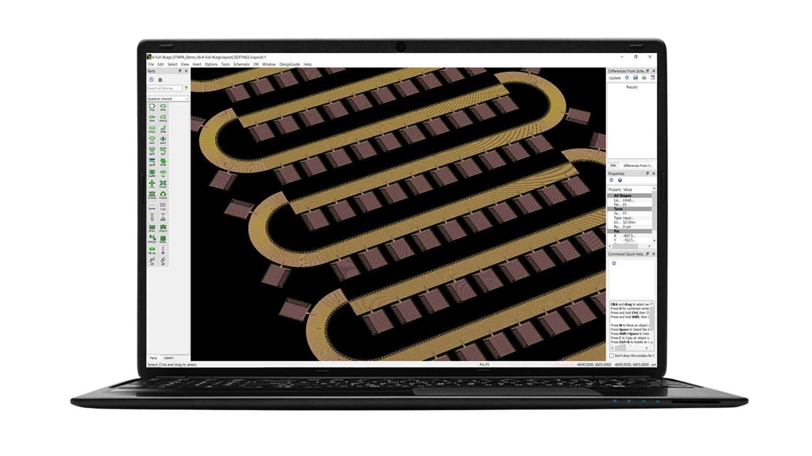
QuantumPro is the EDA industry's first integrated workflow tailored for the seamless design of superconducting qubits.
Advanced Design System (ADS) includes a library of quantum layout components.
Complex product designs need massive and time-consuming simulations. Keysight Design Cloud leverages High-Performance Computing (HPC) technologies that let you run parallel simulations in the cloud, cluster, or server to reduce simulation time and expedite time-to-market significantly.
This webinar explores how Quantum EDA techniques, tailored to the unique requirements of quantum circuits, can facilitate the design process by providing tools for simulation, verification, and optimization.
blogs
Quantum EDA tools help engineers design, simulate, analyze, and optimize superconducting quantum hardware within an integrated workflow. From schematic capture and layout creation to electromagnetic (EM) analysis, nonlinear circuit simulation, quantum parameter extraction, and system-level modeling, EDA software enables designers to evaluate performance before fabrication.
A typical superconducting quantum design workflow begins with defining the qubit architecture and creating schematics and layouts. Engineers then perform electromagnetic simulations to extract quantum parameters such as frequencies, coupling strengths, and participation factors. Next, circuit simulations are used to evaluate nonlinear quantum behavior, followed by system-level simulations that model time-domain experiments such as Rabi and Ramsey sequences. Design iterations continue until performance targets are achieved, after which the design moves to fabrication, packaging, and hardware validation. Quantum EDA platforms streamline this process by connecting these workflows in a unified environment.
EDA tools enable quantum engineering teams to shorten design cycles, reduce fabrication iterations, and improve first-pass success rates. By combining electromagnetic, circuit, and quantum-level simulations, designers can gain deeper insight into qubit performance, amplifier behavior, coupling effects, and package interactions before building hardware. Integrated quantum workflows also help teams scale designs more efficiently as quantum processors become larger and more complex.
Modern Quantum EDA tools combine electromagnetic solvers, nonlinear circuit simulation, Hamiltonian analysis, and time-dynamics modeling to predict qubit behavior. These capabilities allow engineers to simulate qubit frequencies, anharmonicity, coupling mechanisms, energy levels, and experimental pulse sequences. System-level analysis can model real-world experiments such as Rabi and Ramsey measurements, helping designers understand how qubits will behave under operating conditions before fabrication and testing.
Superconducting quantum devices are highly sensitive to geometry, material properties, fabrication variations, packaging effects, and environmental noise. Accurately predicting loss mechanisms, parasitic modes, thermal photon leakage, and nonlinear behavior requires advanced multiphysics and quantum-aware simulation techniques. Quantum EDA tools address these challenges by combining full-wave EM analysis, nonlinear quantum circuit simulation, quantum parameter extraction, and cryogenic system modeling to provide a more complete understanding of device performance.
Talk to our team to find the right solution for your design needs, get a personalized quote, or request a free trial.
您希望搜索哪方面的内容?