这是您想要的页面.
查看搜索结果:
Choose a country or area to see content specific to your location


语言
参数测试解决方案 晶圆级测试系统用于参数验证
型号:NX5402A
上一页
- 概述
- 选项
- 附件
- 软件
- 支持
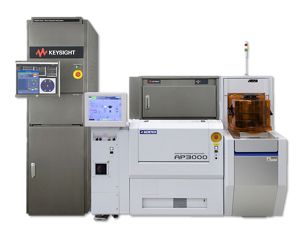
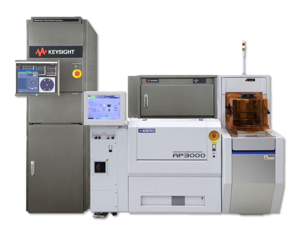
硅光子学晶圆测试系统
NX5402A硅光子学晶圆测试系统配备全自动晶圆探针台,提供批量生产测试所需的全部功能,例如晶圆级测试(WAT)或工艺控制监控(PCM)测试。
-
其他特性
单次通过的光学与电气测试
-
最大测量引脚数
12(光纤输入),12(光纤输出),30(电信号)
-
最小电压测量分辨率
不适用
-
最小电流测量分辨率
不适用
准备报价
了解包含内容,探索是德科技提供的可用升级选项。
关键性能
- 具备光电测试功能的全自动晶圆探针台一体化解决方案
- 针对复杂且大规模的光学与电气测量实现自动化单次测试
- 具备量产就绪能力,支持SECS /GEM工厂自动化 、安全联锁及洁净室就绪功能
- 通过 优化光纤对准与多通道光电测试架构实现高吞吐量测试
- 是德科技的进阶 子校准技术,确保系统性能
- 专属支持模式,确保生产环境的高系统可用性
- 是德科技开发的纤维对准与定位系统
- 领先的PathWave 测试软件,集成是德科技SPECS
- 通过内置自动系统诊断实现可靠的性能监控
- 自动化多配方执行软件,支持多个配方以批处理模式运行
服务 支持
通过精心策划的支持方案、优先响应机制和快速周转时间,实现高效创新。
获取可预测的租赁式订阅服务和全生命周期管理解决方案——助您更快达成业务目标。
KeysightCare ,享受卓越服务,获得专属技术响应等更多权益。
确保您的测试系统符合规格要求,并满足本地及全球标准。
通过内部讲师指导的培训和在线学习,快速掌握测量技能。
下载是德科技软件或将您的软件更新至最新版本。
通过选择产品开始报价
请选择下面的一种配置