


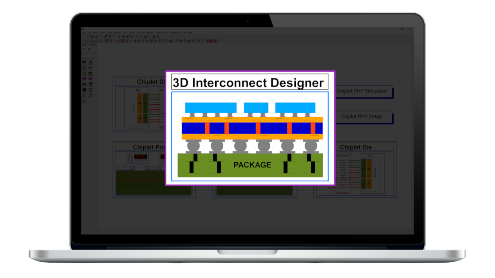
Why Use Chiplet 3D Interconnect Designer
Early design exploration for advanced chiplet architectures.
Advanced packaging has become the primary scaling engine for performance, bandwidth, and system integration, driven by AI and data center workloads. The rapid adoption of 2.5D, 3D, and emerging 3.5D packaging technologies introduces significantly higher integration density, enabled by advanced techniques such as hybrid bonding, TSV-based stacking, silicon interposers, and redistribution layers (RDL). At the same time, standardized die-to-die interconnect protocols are emerging, which bring both opportunities for interoperability and challenges in multi-vendor chiplet integration. At these data rates, package interconnects behave like transmission lines and exhibit strong coupling effects throughout the structure. This fundamentally changes the role of packaging—from a back-end assembly step to an integral part of the electrical design. The Chiplet 3D Interconnect Designer feature simplifies complex chiplet integration by enabling early design validation and reducing costly layout iterations.
Key Capabilities

Design optimized chiplet interconnect channels quickly.

Evaluate alternatives before full package implementation.

Leverage standards-driven bump map generation.

Analyze hatched and waffle ground planes.

Accelerate early channel performance investigations.

Connect directly with Chiplet PHY Designer.
Resources to Get You Started
Introduction to Chiplet 3D Interconnect Designer
Learn the fundamental concepts of chiplet-based design and how to begin creating, analyzing, and optimizing die-to-die interconnect channels. The introduction demonstrates the software's guided workflow, helping new users understand interconnect architecture exploration, bump map configuration, channel modeling, and performance evaluation. By walking through key design tasks and visualization tools, the video provides a practical starting point for engineers who are new to chiplet and advanced package design workflows.
Bootcamps
Designing with Chiplets and Advanced Packaging to build system-on-chips (SoCs)

blogs
How to Streamline Your Advanced Package (Chiplet, 3DIC) Interconnect Designs

技术概述
Keysight EDA Electronic Design Automation Software

白皮书
Mitigating Signal Integrity Challenges in High-Speed Chiplet Designs
白皮书
UCIe vs. BoW: Practical Insights for Choosing the Right Chiplet Standards
Have Questions? We've Got Answers
Chiplet 3D Interconnect Designer is a design and optimization environment for die-to-die interconnect channels used in chiplet-based systems. It helps engineers evaluate and optimize interconnect performance before package layout completion.
The solution supports chiplet interconnect design on silicon bridges, organic bridges, and interposers, enabling efficient exploration of advanced packaging architectures.
Yes. Chiplet 3D Interconnect Designer includes standards-driven bump maps for emerging die-to-die communication standards such as UCIe and BoW.
By enabling early architecture exploration and fast channel modeling, engineers can identify performance limitations and optimize interconnects before committing to a detailed package implementation.
Yes. The solution integrates directly with Chiplet PHY Designer, creating a streamlined workflow from interconnect design through channel and PHY validation.