

Why Use Keysight Photonic Designer
Built on the Keysight Photonic Design Automation platform, this tool provides a seamless, end-to-end workflow for electrical-optical-electrical (EOE) design, from concept to wafer-level characterization.
The Photonic Designer integrates cutting-edge physics-based simulation technology for unmatched accuracy and reliability, making it ideal for both seasoned professionals and newcomers to photonics. The tool is embedded within the Advanced Design System (ADS), offering a streamlined experience that simplifies complex design processes while saving time and resources.
Advanced Design System (ADS)
EDA platform for Photonic Designer.
Keysight ADS is the premier electronic design automation (EDA) platform for the design of physical layer components that enables engineers to design, analyze, and optimize the critical components that power today's most advanced commercial and defense systems. The base platform contains powerful 3D physical layout and verification, data display, optimization, statistical analysis, Python scripting automation, and AI-Assisted design tools. High-Performance Computing (HPC) options can significantly accelerate simulation times. Additional simulation capabilities such as nonlinear circuit, electromagnetic (EM), electrothermal (ETH) and system provide engineering teams with a choice of value-packed, preconfigured combinations of software modules built for specific design workflows: RF/Microwave, High-speed Digital, Power Electronics, Photonic and Quantum.


Key Capabilties

Optical finite difference eigenmode (OFDE) solver

Linear frequency domain simulator

AC simulations for small signal AC analysis

DC simulations for DC operating point calculations

Transient / convolution nonlinear circuit simulator

Harmonic balance nonlinear circuit simulator

Circuit envelope nonlinear circuit simulator
Optimizing a PIN Photodetector Model
The rapid advancement in photonic integrated circuits (PICs) calls for sophisticated tools that streamline the design and validation process. Keysight Photonic Designer represents a leading-edge photonic design automation (PDA) solution, purpose-built to address the demands of next-generation photonic integrated circuit (PIC) design.

Using the Optical Mode Solver from Keysight Photonic Designer
Watch a comprehensive overview of the optical finite difference eigenmode (OFDE) solver available within Keysight Photonic Designer. The mode solver is a powerful 2D cross-sectional tool designed to calculate optical modes for waveguides and directional couplers, enabling engineers to analyze and optimize photonic designs.
Integrated PIC and Device Design Workflow
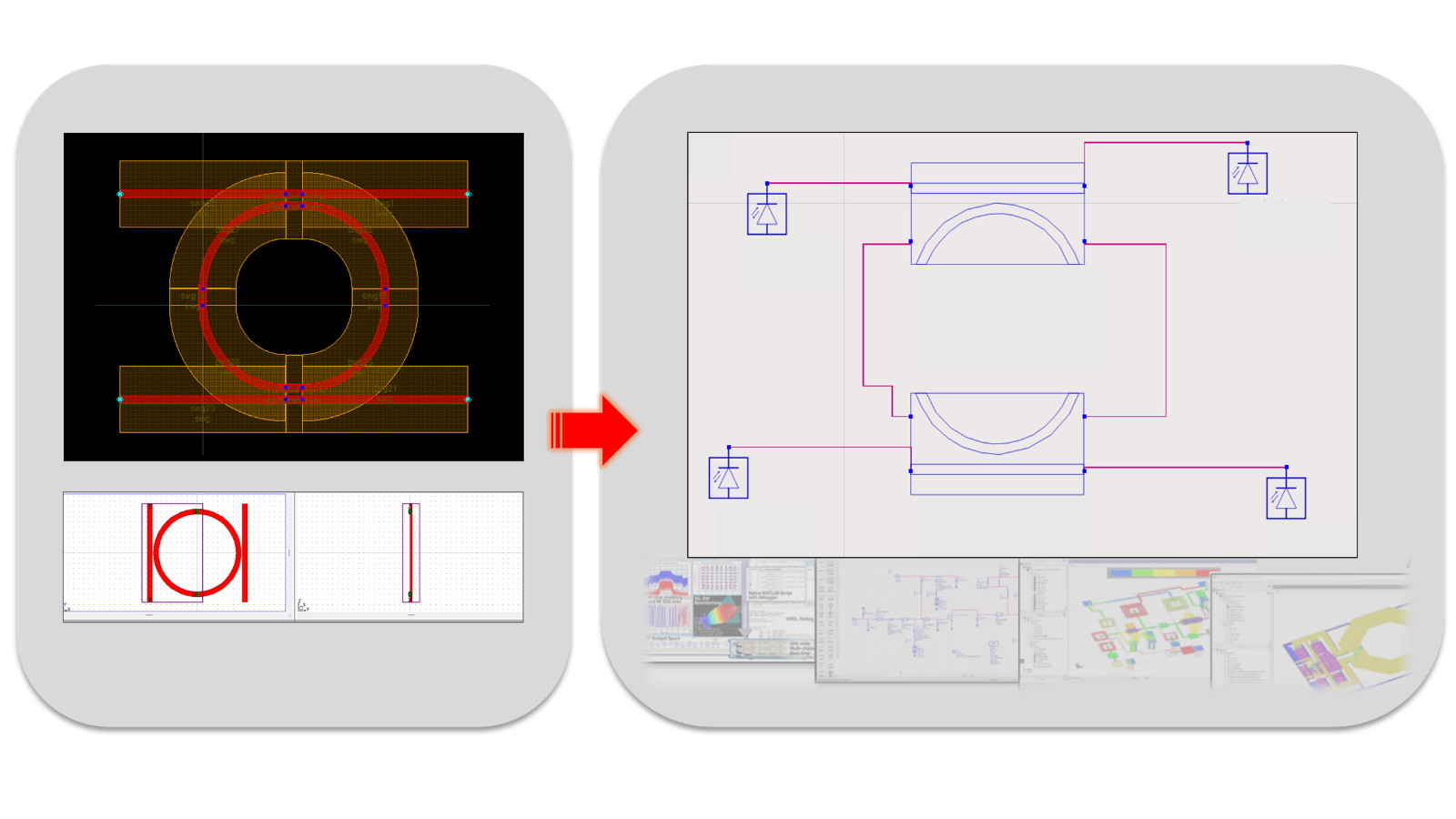
Photonic integrated circuit development often requires both device-level analysis and circuit-level design. ADS Photonic Designer and RSoft Photonic Device Tools provide a connected environment that links electromagnetic and optical device simulation with PIC schematic capture, layout, and circuit analysis. Engineers can evaluate device behavior, generate reusable models, and assess system-level impact within a consistent design flow.

Resources to Get You Started
End-to-End Electro-Optical Co-Design for Optical Interconnects
Keysight enables a patent-protected Electrical–Optical–Electrical (EOE) design workflow for next-generation optical interconnects such as Linear Pluggable Optics (LPO), Co-Packaged Optics (CPO), On-Board Optics (OBO), and Near-Package Optics (NPO). By combining Keysight System Designer for Ethernet with Keysight Photonic Designer inside Keysight Advanced Design System, engineers can simulate the complete Ethernet link from electrical drivers and photonic transmitters, through the optical channel, to the electrical receiver.
The solution supports multi-channel optical links, full-duplex simulations with forward and backward propagating signals, and wavelength-division multiplexing (WDM) analysis. Optical circuits used at the system level can be directly reused for PIC implementation, while device-level optimization can be performed using RSoft Photonic Device Tools enabling a unified system-to-circuit-to-device design flow for photonic systems.
End-to-End Co-Design for Ethernet: Bridging Photonics and Electronics with EOE Simulation
As data rates continue to scale in modern data centers and AI-driven infrastructure, traditional siloed design approaches are no longer sufficient. This on-demand webinar introduces a unified electrical-optical-electrical (EOE) simulation workflow that bridges electronic and photonic domains using Photonic Designer and System Designer for Ethernet within the Keysight Advanced Design System (ADS).


应用文章
End-to-End Electrical-Optical-Electrical Flow in Keysight ADS

应用文章
Optimizing Photodetector Model to a Silicon Photonics Foundry Process
技术概述
Keysight EDA Electronic Design Automation Software
Have Questions? We've Got Answers
Photonics is the science of generating, controlling, and detecting light (photons). Unlike electronics, which use electrons to carry signals, photonics uses photons—enabling higher data rates, lower signal loss, and resistance to electromagnetic interference.
Photonic Design Automation (PDA) is a suite of tools for designing, simulating, and validating photonic integrated circuits (PICs). It helps model optical behavior and supports layout-to-fabrication workflows.
Photonic components are sensitive to geometric and material variations. Accurate simulation reduces prototyping costs, ensures performance, and speeds up development cycles.
Common simulation methods include:
- FDTD: Accurate for broadband and complex nanostructures.
- FEM: Ideal for irregular geometries and high index contrasts.
- EME: Efficient for waveguide-based passive structures.
- BPM: Fast for large-scale, gradual structures.
- OFDE: Optimized for frequency-domain analysis of full circuits.
Designers often combine these methods to balance speed and accuracy.
Photonic integrated circuits (PICs) use light instead of electricity for signal transmission, enabling faster speeds, lower power, and higher bandwidth in applications like communications and sensing.
PDA tools enable precise design and simulation of silicon photonics using CMOS-compatible processes. They support accurate modeling, foundry-specific rules, and hybrid electro-photonic integration.
PICs are used in high-speed data communication, LiDAR, quantum computing, biomedical sensing, and RF signal processing, offering compact, efficient, and scalable optical systems.
Co-simulation models both photonic and electronic components in a unified environment, essential for designing integrated systems like modulators and transceivers.
A photonic layout defines the physical structure of a circuit for fabrication, including waveguides and components. Adhering to foundry rules ensures manufacturability and performance.
Key challenges include minimizing optical losses, tight fabrication tolerances, electro-photonic integration, and adherence to foundry-specific constraints.
Foundry support ensures compatibility with process design kits (PDKs), enabling accurate, fabrication-ready designs with higher yield and fewer design iterations.