


Why Use Photonic Foundry PDK Library
Prototype, optimize, and validate photonic integrated circuits using foundry-ready design workflows.
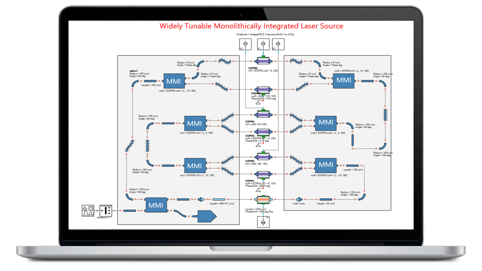
Developing photonic integrated circuits (PICs) requires efficient collaboration between circuit design, layout implementation, and foundry manufacturing requirements. This solution provides a powerful Process Design Kit (PDK) environment that enables engineers to rapidly prototype and optimize application-specific photonic integrated circuits using foundry-qualified building blocks and simulation models. Its unique layout-aware schematic-driven methodology bridges the gap between schematic capture and physical implementation, automatically incorporating layout information, waveguide routing, and fabrication constraints into the design process. By integrating circuit simulation with industry-leading photonic layout tools, engineers can evaluate performance, analyze fabrication tolerances, optimize yield, and prepare manufacturable designs more efficiently. The result is faster development cycles, lower design risk, improved design accuracy, and streamlined transition from concept to fabrication for advanced photonic devices and systems.
Key Capabilities

Utilize validated foundry building blocks and models.

Incorporate physical layout directly into simulations.

Generate intelligent optical interconnects automatically.

Rapidly develop application-specific photonic circuits.

Evaluate fabrication tolerances and process variations.

Export designs to leading PIC layout platforms.
Resources to Get You Started
blogs
Completing Keysight's End-to-End Photonic Design Workflow
Brochures
Photonic Design Automation for Components, Systems & Networks

Have Questions? We've Got Answers
A photonic Process Design Kit (PDK) provides foundry-specific building blocks, device models, and design rules that enable engineers to create manufacturable photonic integrated circuits efficiently.
The methodology combines schematic capture with physical layout information, enabling designers to account for component placement, routing, packaging constraints, and fabrication requirements during simulation.
The platform supports multiple integrated photonics technologies, including indium phosphide (InP), silicon photonics, silicon nitride, and polymer-based photonic platforms.
Yes. Designs can be exported to industry-standard photonic layout environments such as PhoeniX OptoDesigner, IPKISS, and Nazca for layout refinement, verification, packaging, and GDSII generation.
By combining validated foundry models, layout-aware simulation, automated routing, yield analysis, and fabrication-aware optimization, engineers can identify issues earlier and improve first-pass design success.