


Why Use Quantum Layout
Build simulation-ready quantum-chip layouts efficiently.
Quantum Layout provides reusable components for creating qubits, resonators, coplanar-waveguide structures, peripheral circuitry, and distributed structures used in quantum amplifiers—helping teams create consistent, simulation-ready designs with fewer manual layout steps.
Key Capabilities

Resonators and qubits for crafting the layout of QPUs, peripheral circuits, and developing Quantum Amplifiers (QAs).

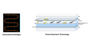
Automated airbridges eliminate the hassle of dealing with unwanted CPW line modes.

Multilayer layout technology enables you to scale up the number of qubits.

Manage complex signal interactions and avoid issues like crosstalk and phase mismatches.
Jump-Start your Development with the Preset Quantum Technology
Our advanced quantum technology jump-starts your development process, while automated airbridges eliminate the hassle of dealing with unwanted CPW line modes. Plus, our multilayer technology makes it easy to scale up the number of qubits.


Scale-Up the Number of Qubits
Increasing the number of qubits is one of the biggest challenges in quantum computing. To tackle this, we often stack multiple wafers on top of each other. This method helps us make better use of the space on the wafers for qubits, while routing the signals between them on a different layer. However, this multilayer quantum technology requires careful planning and precise connections. Our Layout solution supports this multilayer technology, empowering you to scale up the number of qubits and take on this challenge.
Manage the Layout Complexity of Quantum Amplifiers
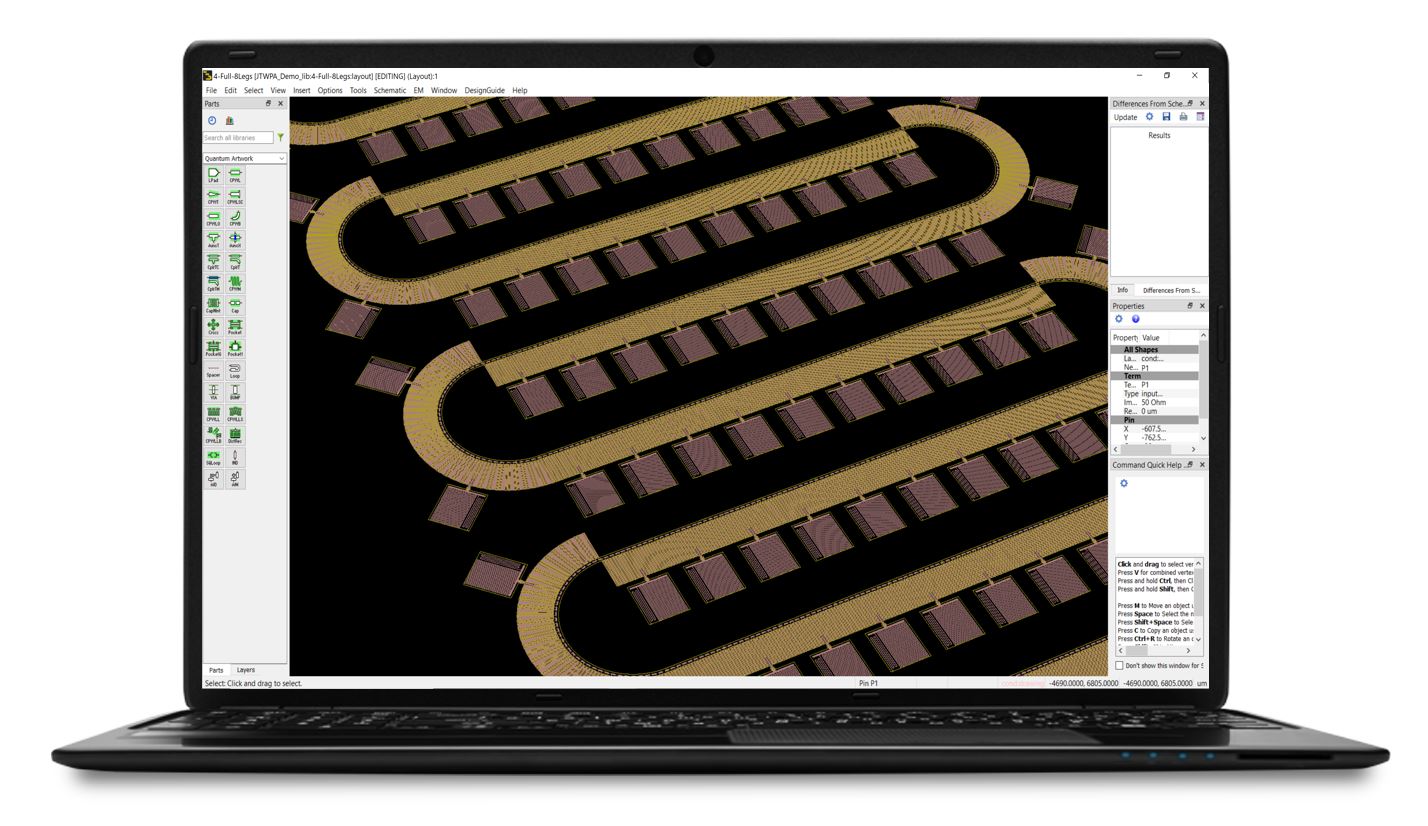
The design of quantum amplifiers can range from simple setups with just a few Josephson junctions (JJs) to complex structures with thousands of JJs, like Josephson Traveling Wave Parametric Amplifiers (JTWPAs). Basic amplifier designs with fewer JJs typically focus on efficient coupling between quantum elements and optimal signal paths. In contrast, JTWPAs, with their large number of JJs, require careful layout strategies to manage complex signal interactions and avoid issues like crosstalk and phase mismatches. Designing these advanced amplifiers involves intricate arrangements of JJs and resonators, meticulously crafted to ensure precise control over signal propagation and amplification. The great news is that we have components specifically for distributed loaded coplanar waveguide artworks, which can be utilized in the development of traveling wave quantum structures such as JTWPAs, helping you navigate this challenge.


Resources to Get You Started
Build Your Quantum Chip Easily in ADS
Layout your quantum designs in ADS.
Advanced Design System (ADS) includes a library of quantum layout components. The library encompasses numerous frequently used quantum designs including transmons and co-planar waveguide (CPW) meanderline resonators. Its introduction facilitates the creation of quantum chips from within the ADS layout environment, with each geometrical feature of the chip being represented as a parameterized object that can be easily adjusted and optimized. The CPW components within the library have built-in airbridges that play a crucial role in preventing the propagation of the CPW common mode.
Have Questions? We've Got Answers
Quantum circuit layout is the process of creating the physical geometry of superconducting quantum devices, including qubits, resonators, couplers, control lines, and readout structures. The layout directly affects critical performance metrics such as qubit frequency, coupling strength, crosstalk, radiation loss, and manufacturability. Because superconducting qubits are highly sensitive to their physical environment, an optimized layout is essential for achieving high-fidelity quantum operations and scalable quantum processor designs. Keysight's ADS Quantum Layout provides parameterized quantum components that help engineers efficiently create and optimize these structures.
A superconducting quantum chip typically contains transmon qubits, coplanar waveguide (CPW) resonators, couplers, readout resonators, control lines, airbridges, and grounding structures. As quantum processors grow in complexity, layouts may also include packaging interfaces, flip-chip connections, and 3D cavity structures. Keysight notes that its quantum layout library includes commonly used structures such as transmons and CPW meander-line resonators, enabling designers to rapidly build and customize quantum chips.
Parameterized layout cells allow engineers to adjust geometric properties such as qubit pad dimensions, resonator lengths, coupling gaps, and transmission line widths without redrawing the design. This enables rapid design exploration and optimization while maintaining consistency across the project. By linking geometry directly to simulation workflows, engineers can quickly evaluate how physical changes affect frequencies, coupling, and overall quantum performance. Keysight's quantum layout environment uses parameterized objects to streamline design iterations and accelerate optimization.
The physical arrangement of structures on a quantum chip strongly influences qubit coherence, coupling, crosstalk, and loss mechanisms. Poor layout choices can introduce unwanted electromagnetic modes, excessive coupling between neighboring devices, radiation loss, and fabrication sensitivities. Layout optimization helps ensure that qubits achieve target frequencies while minimizing interference from nearby structures. Modern Quantum EDA workflows combine layout creation with electromagnetic simulation to evaluate these effects before fabrication.
Modern Quantum EDA platforms connect layout design directly to electromagnetic and circuit simulation workflows. Engineers can create a layout, perform EM analysis to extract quantum parameters, and then use those parameters in circuit and system-level simulations without moving between disconnected tools. This integrated approach reduces errors, shortens design cycles, and improves confidence in simulation results. Keysight's QuantumPro and ADS Quantum Layout environments provide a unified workflow spanning layout, EM analysis, quantum parameter extraction, and circuit simulation for superconducting quantum hardware.