


Why Use 3D Interconnect Designer
Comprehensive design for advanced packages and heterogeneous integration.
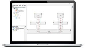
The 3D Interconnect Designer is a design tool purpose-built for advanced packaging. If offers a smart, unified workflow for designing 2.5D, die-to-die, and 3D stacked-die architectures. The 3D Interconnect Designer supports accurate modeling of complex interconnect structures including those with hatched ground planes, while supporting emerging chiplet standards such as UCIe and Bow, enabling standards-aware design and interoperability across multi-vendor ecosystem. The tool offers a wide variety of interconnect models including microbumps, solder balls, vias, and multi-lane transmission line models that all are validated through close correlation between simulation and measurement, ensuring high confidence in result. The 3D Interconnect Design (W3510E) that is integrated to Chiplet PHY Designer is a special version tailored for Chiplet applications for die-to-die interconnects for UCIe and BoW standards. The standalone 3D Interconnect Designer (W9100E) is a generic version that is not limited only for Chiplet but applicable for any 3D interconnect designs such as chip on board or package on board or full stack 3D designs.
Key Capabilities

Model complete package and interconnect structures accurately.

Optimize vias, micro-bumps, and solder ball connections.

Design and analyze complex 3DIC architectures.

Support hatched and waffle ground structures.

Develop advanced multi-die system architectures efficiently.

Works with ADS and external design tools.
Resources to Get You Started
3D Interconnect Designer for Advanced Packaging Workflows
Learn how to model, analyze, and optimize complex interconnect structures used in chiplets, 2.5D packages, and 3DIC designs. The demonstration showcases workflow-driven design exploration, detailed modeling of vias, micro-bumps, transmission lines, and ground structures, while illustrating how engineers can evaluate performance tradeoffs before fabrication. Viewers will also gain insight into heterogeneous integration workflows, advanced package validation, and techniques for reducing design risk while accelerating development of next-generation semiconductor systems.
应用文章
AI-Assisted Automation for Advanced Packaging

Webinars
How To Design Advanced Package Interconnects Without Hatched Ground Simulation Bottlenecks

技术概述
Keysight EDA Electronic Design Automation Software
How-To Videos
Quick-Start Video for 3D Interconnect Designer
Product Tours
Introduction to Chiplet 3D Interconnect Designer
Product Tours
3D Interconnect Designer 2026 U1 Highlights
样机
3D Interconnect Designer for Advanced Packaging Workflows
解决方案概述
3D Interconnect Designer: Physically Accurate Design and Exploration of Advanced 2.5D and 3D Interconnects
白皮书
Computationally Efficient Design and Optimization
应用文章
Practical Modeling of 3D Interconnects with Hatched Ground Planes in Silicon Interposer Bridges, and Flex PCBs
Have Questions? We've Got Answers
3D Interconnect Designer is a modeling and optimization solution for advanced package, chiplet, 3DIC, and PCB interconnect design. It helps engineers evaluate and optimize complex interconnect structures before fabrication.
The software supports modeling of vias, micro-bumps, solder balls, transmission lines, chiplets, stacked die architectures, advanced packages, and PCB interconnects.
No. While it supports chiplet designs, the solution is intended for a broader range of advanced packaging applications, including heterogeneous integration, stacked die, and complete 3DIC systems.
Engineers can explore design alternatives, optimize interconnect structures, and identify performance issues earlier in the workflow, reducing costly redesigns and accelerating development schedules.
Yes. The solution integrates with ADS and can also be used within external EDA workflows, providing flexibility for existing design environments and processes.