
PathWave Advanced Design System (ADS)
解决方案概述
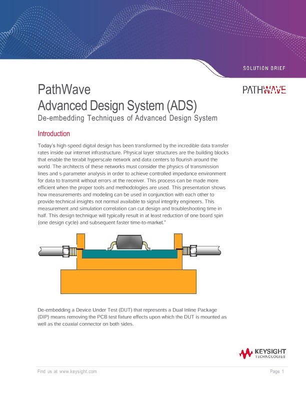
Today’s high-speed digital design has been transformed by the incredible data transfer rates inside our internet infrastructure. Physical layer structures are the building blocks that enable the terabit hyperscale network and data centers to flourish around the world. The architects of these networks must consider the physics of transmission lines and s-parameter analysis in order to achieve controlled impedance environment for data to transmit without errors at the receiver. This process can be made more efficient when the proper tools and methodologies are used. This presentation shows how measurements and modeling can be used in conjunction with each other to provide technical insights not normal available to signal integrity engineers. This measurement and simulation correlation can cut design and troubleshooting time in half. This design technique will typically result in at least reduction of one board spin (one design cycle) and subsequent faster time-to-market.”