
HMMC-5645 40 GHz Doubler
技术资料
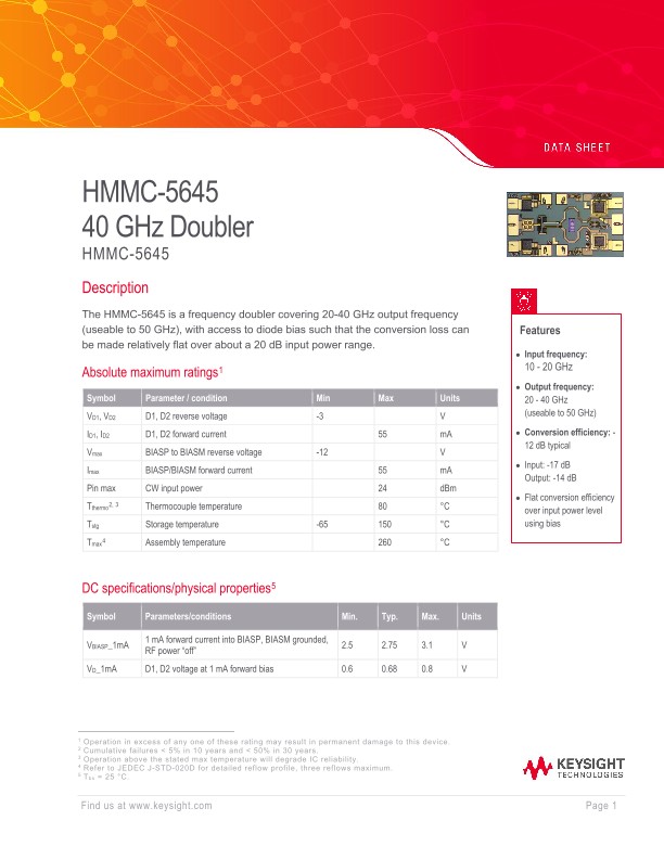
HMMC-5645
Description
The HMMC-5645 is a frequency doubler covering 20-40 GHz output frequency (useable to 50 GHz), with access to diode bias such that the conversion loss can be made relatively flat over about a 20 dB input power range.
Frequency-domain AC specifications1
Symbol |
Parameters/conditions |
Min. |
Typ. |
Max. |
Units |
CE20 |
Conversion efficiency, 10 GHz input |
-13.0 |
-11 |
-9.5 |
dB |
CE34 |
Conversion efficiency, 17 GHz input |
-13.6 |
-12.5 |
-11 |
dB |
CE50 |
Conversion efficiency, 25 GHz input |
-13.6 |
-12.5 |
-8 |
dB |
Feedthru10 |
X1 Feedthru, 10 GHz |
10 |
13.5 |
15 |
dBc |
Feedthru17 |
X1 Feedthru, 17 GHz |
18 |
24 |
29 |
dBc |
Feedthru25 |
X1 Feedthru, 25 GHz |
21 |
25 |
32 |
dBc |
ESD Sensitivity2
Symbol |
Parameters/conditions |
Min. |
Max. |
Units |
D1, D2 |
HBM3 |
-400 |
+1700 |
V |
RF input |
HBM3 |
-700 |
+700 |
V |
RF output |
HBM3 |
-400 |
+400 |
V |
BIASP, BIASM |
HBM3 |
-500 |
+500 |
V |
Applications
The HMMC-5645 can be used as a general-purpose frequency doubler. If flat conversion loss vs. input level is needed, access to the diodes is provided for biasing in an optimal fashion.
Operation
The circuit is a full wave rectifier, using diodes and a balun. Double diode junctions are used to increase power handling.
Recommended Biasing
Nominal Bias
In non-critical applications, BIASP and BIASM will simply be connected to ground with bond wires. Where flat conversion loss vs. input level is desired, BIASP and BIASM will be connected to voltage sources which have been empirically designed to minimize conversion loss variations over the input range. “Dummy” diodes D1 and D2 are provided to help create the desired bias voltages via off-chip analog circuitry, and will be useful to help minimize performance changes due to temperature variations. BIASP and/or BIASM can also be used to peak up conversion efficiency at any specific use condition.
Bias Sequencing
There is no critical order involved with biasing, simply apply bias in any convenient manner. It is acceptable to ground one side and apply bias only to the other side if desired; or a symmetrical +/- bias can be used.
Assembly Techniques
Die attach should be done with conductive epoxy. Gold thermosonic bonding is recommended for all bonds. The top and bottom metallization is gold.
ESD Warning
III-V MMICs are ESD sensitive. Damage from ESD events can significantly affect III-IV MMIC performance and reliability. Preventative ESD measures must be employed in all aspects of storage, handling, and assembly, in compliance with the Keysight ESD Control Program. Information on the Keysight ESD Control Program can be found at:
http://emg.communications.keysight.com/quality/esd/
For information on ESD precautions during die attach and bonding, please refer to Keysight application note #54, "III-V MMIC ESD, Die Attach and Bonding Guidelines" pub # 5991-3484.
Reliability Warning
The chip must be die-attached to a substantial thermal mass, such as an aluminum microcircuit or PC board trace with plenty of copper and vias to ground planes. The backside of the chip must be kept at or below 75 °C. The maximum allowed input power is 24 dBm, with 3 V bias from BIASP to BIASM (or less). Failure to comply with these requirements will result in reduced chip lifetime, or immediate catastrophic failure.
RoHS Compliance
This part is RoHS compliant, meeting the requirements of the EU Restriction of Hazardous Substances Directive 2002/95/EC, commonly known as RoHS. Six substances are regulated: lead, mercury, cadmium, chromium VI (hexavalent chromium), polybrominated biphenyls (PBB), and polybrominated biphenyl ethers (PBDE). RoHS compliance requires that any residual concentration of these substances is below the Directive’s maximum concentration values (MCV): cadmium 100ppm by weight and all others 1000 ppm by weight.