
Practical RF Amplifier Design Using the Available Gain Procedure and the Advanced Design System EM
白皮书
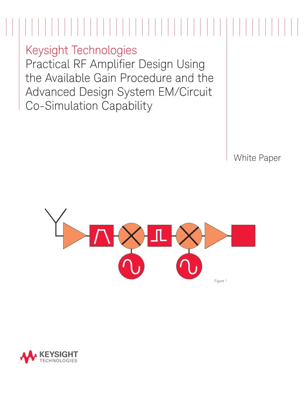
This article features a low noise RF amplifier design method for an 802.11b receiver application containing a Avago ATF54143 PHEMT transistor. ADS design tools are used such that the techniques presented remove much of the guesswork from the design process. Design speed and cost, along with RF performance, are of utmost importance for most RF designs, thus, one of the main objectives is to yield an amplifier design that works with the first PCB pass. If successful, multiple PCB layouts are avoided, which saves design cost and time. This RF amplifier design procedure is considered successful even if some of the lumped component values must be adjusted slightly to get the desired RF performance (so long as the layout does not have to be modified to have a working circuit).
The low noise RF amplifier design will also be considered successful even if the model prediction doesn’t agree exactly with measured results, but the resulting circuit still meets the design criteria and specifications. In this white paper, the RF amplifier design is illustrated from start to finish, with construction of a printed circuit board and measurement results.