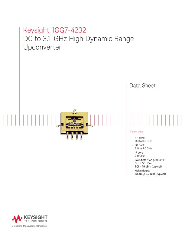
1GG7-4232 DC to 3.1 GHz High Dynamic Range Upconverter
技术资料
Keysight 1GG7-4232
DC to 3.1 GHz High Dynamic Range Upconverter
Features
- RF port: DC to 3.1 GHz
- LO port: 3.9 to 7.0 GHz
- IF port: 3.9 GHz
- Low distortion products:
SHI > 53 dBm
TOI = 19 dBm (typical)
- Noise figure: 13 dB @ 2.7 GHz (typical)
Description
The 1GG7-4232 is a packaged MMIC double balanced ring diode mixer with on-chip LO and IF amplifiers. The LO amp is a limiting buffer amp that allows the device to be driven by relatively low LO drive levels. The IF amp is a low noise amp that helps improve system noise figure. The 1GG7-4232 is fabricated using the Keysight Technologies, Inc. GaAs diode process. The device is mounted in a 7-lead glass/metallized Gull-wing lead style flat-pac.
Applications
The 1GG7-4232 double balanced mixer is ideal for upconverting DC to 3.1 GHz signals to an IF of 3.9 GHz. The high dynamic range makes this an attractive first converter in applications where both low distortion and low noise are important.
Biasing and Operation
The 1GG7-4232 can be self–biased by leaving VGG1/2 open, or the bias can be set for optimum TOI operation. For self–bias operation, the 1GG7-4232 can be biased from a single –5.0 volts and a 6.81 Ω resistor. The –5.0 volts is applied directly to VSS1 and indirectly to VSS2 via the 6.81 Ω resistor. The 1GG7-4232 is designed to upconvert a DC to 3.1 GHz signal to an IF frequency of 3.9 GHz. The LO drive is nominally +14 dBm over the range 3.9 to 7.0 GHz. Bypass capacitors are recommended on VSS2 and VGG2. Without these capacitors, some degradation in noise figure may result. 03 | Keysight | 1GG7-4232 DC to 3.1 GHz High Dynamic Range Upconverter - Data Sheet Figure 1. 1GG7-4232 package schematic For optimum bias to achieve the best TOI, VGG1 should be adjusted so that ISS1 is 100 mA, and VGG2 should be adjusted so that ISS2 is 150 mA. The gate bias connections VGG1 and VGG2 will require voltages between –10 and 0 volts to achieve these conditions. The RF port match is optimized in the package through the use of two off-chip compo[1]nents; a series 1 nH inductive bond-wire (LRF) and a shunt 1 pF capacitor (CRF). Figure 3 shows the location of the off-chip components.
Assembly Techniques
This package is compatible with wave-solder or reflow printed circuit board soldering processes. The package backside MUST be DC and RF ground. The leads are gold-plated and should be pre-tinned to facilitate soldering. GaAs MMICs are ESD sensitive. ESD preventive measures must be employed in all aspects of storage, handling, and assembly. MMIC ESD precautions, handling considerations, die attach and bonding methods are critical factors in successful GaAs MMIC performance and reliability. The Keysight Technologies, Inc., GaAs MMIC ESD, Die Attach and Bonding Guidelines - Application Note (5991-3484EN) provides basic information on these subjects.