Choose a country or area to see content specific to your location
您希望搜索哪方面的内容?
Design, model, and validate complex 3D interconnect architectures with a powerful standalone design environment.
Automate transmitter and receiver validation across next-generation I/O, memory, and fabric interfaces.
Strengthen 1.6T network reliability for AI-scale workloads from transceivers to interconnects.
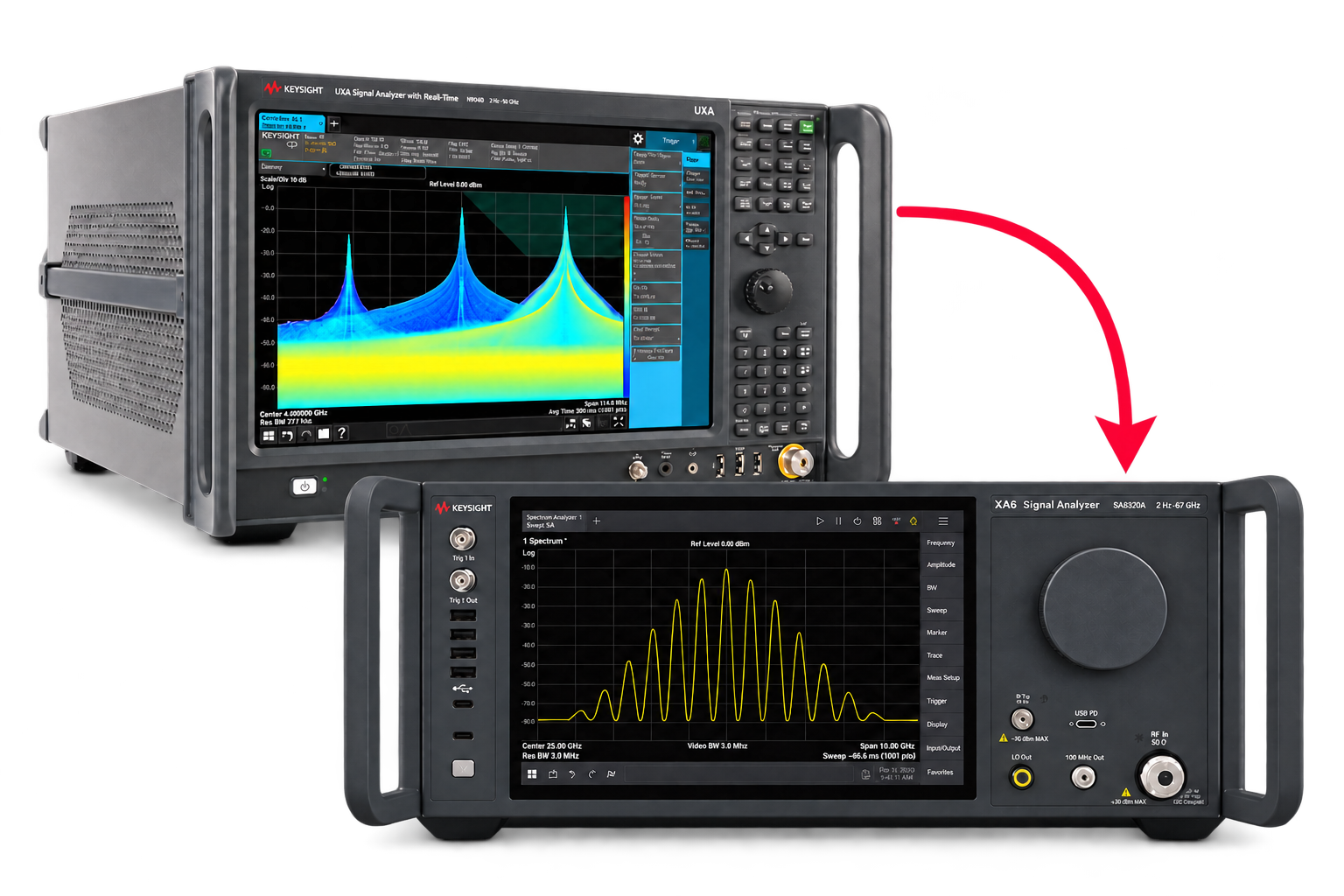
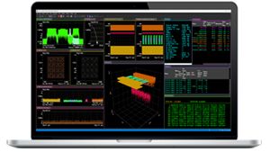
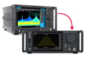
Pair Keysight VSA software with the new XA5 signal analyzer for advanced visualization, demodulation, and analysis — start your 30-day trial today.
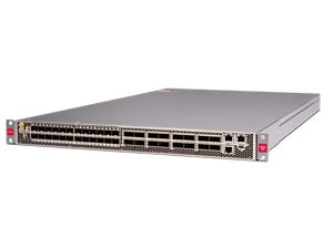
With extra memory and storage, these enhanced NPBs run Keysight's AI security and performance monitoring software and AI stack.
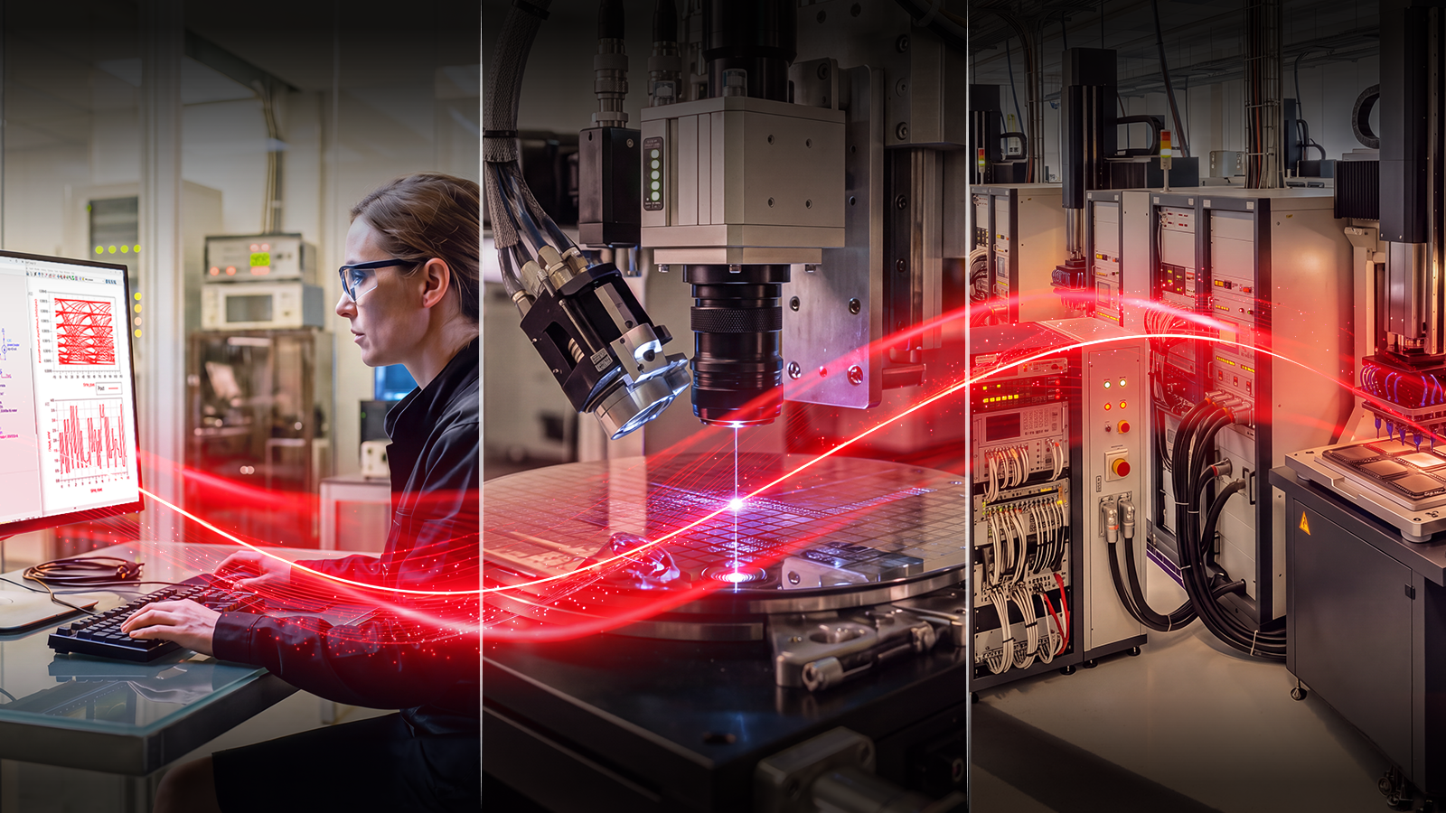
Explore end-to-end workflows spanning IC design, validation, wafer test, and photonics.
Save up to 50% on our latest instruments with eligible Keysight or competitor trade-ins.
Maximize accuracy and performance with precision accessories engineered for Keysight instruments.
Save up to 50% on our latest instruments with eligible Keysight or competitor trade-ins.
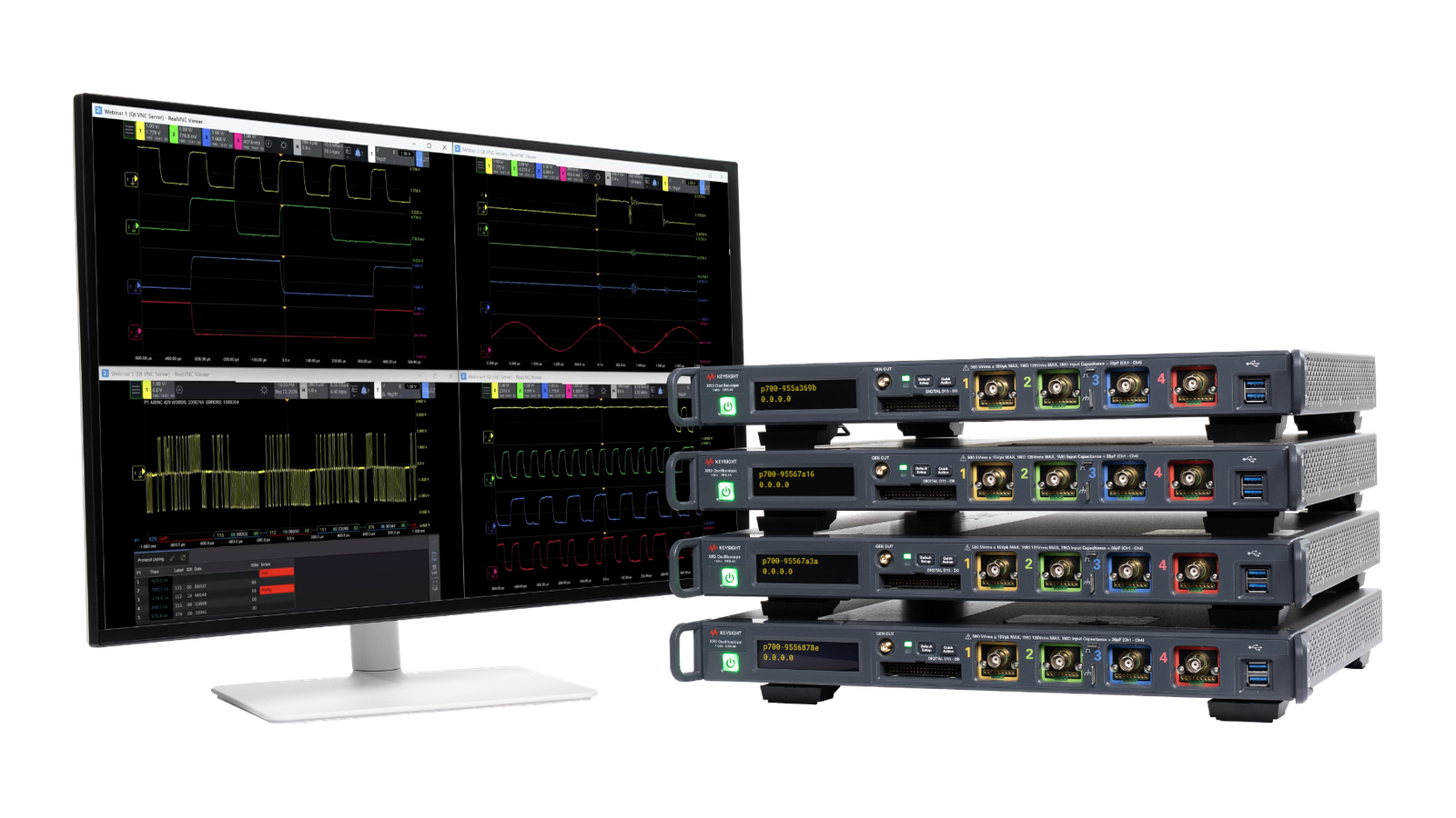
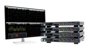
Four channels per 1U of rack space, up to 1 GHz bandwidth, and multi-oscilloscope synchronization.
Purpose-built solutions engineered for the design and test challenges unique to your industry.
Use Cases mapped to every stage of your product lifecycle, from design through operations.
Success Stories
Authoritative application notes, data sheets, reference designs, and test procedures to accelerate design and validation decisions.
Hands‑on bootcamps that teach system design, test methods, and production workflows engineers can apply immediately.
Learning Hub
Explore methodologies, test strategies, and technical resources for designing, validating, and scaling AI systems and networks.
Accelerate measurement, analysis, and modeling workflows from wafer to model.
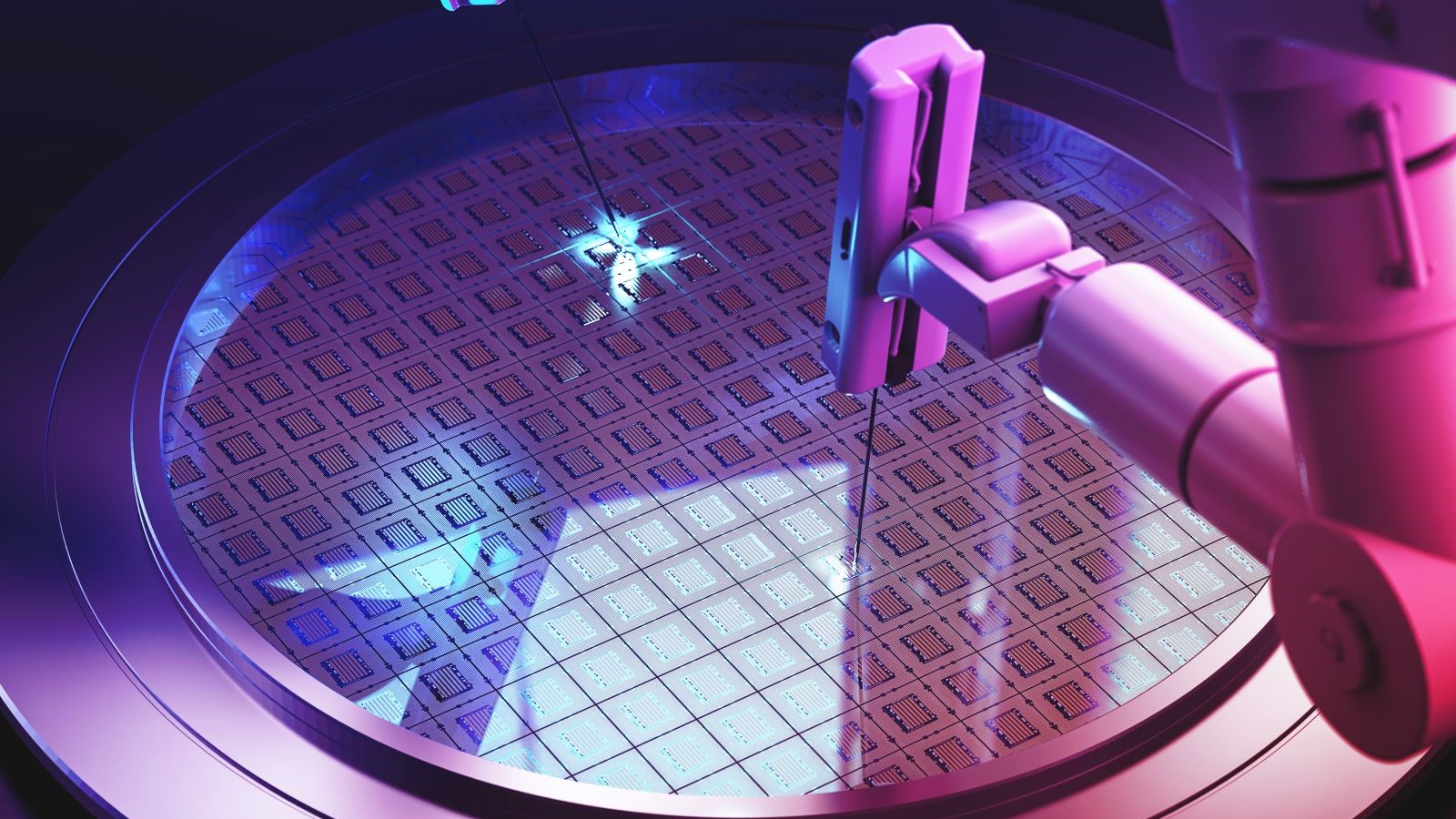
Automate wafer-level characterization and scale measurement productivity.
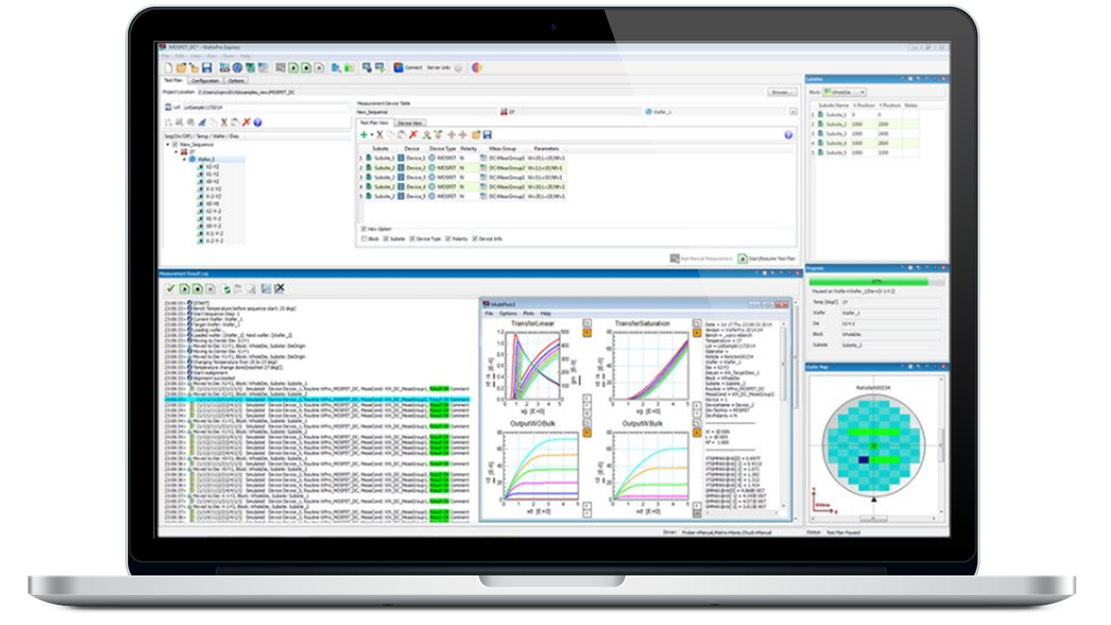
Modern semiconductor technologies require large volumes of accurate measurement data collected across multiple devices, wafers, and test conditions. WaferPro streamlines characterization with automated wafer-level measurements, integrated instrument control, and flexible test plan execution.
By consolidating measurement automation, wafer prober control, and data collection into a single workflow, WaferPro helps characterization teams increase throughput, improve measurement consistency, and accelerate the delivery of high-quality data for device modeling and process development.
Automate complex wafer-level measurement workflows.
Connect and control instruments with built-in drivers.
Works with leading wafer prober platforms.
Develop customized measurements and data analysis.
Synchronize wafer maps and calibration status.
Analyze high-volume measurement data efficiently.
Integrated system with Keysight A-LFNA for 1/f flicker noise, RTN, phase noise, device characterization, and other low-frequency noise measurements.
Integrated system with Keysight SPA for DC parametric measurements.
Integrated Measurement System with Keysight VNA for S-parameters from RF to mmW to THz.
WaferPro enables measurement automation, wafer prober control, and data ready for modeling. Furthermore, your test plans may be easily scaled across your lab. WaferPro provides a unified measurement platform that eliminates the complexity of software integration, allowing an engineer to set up and execute wafer-level measurements of semiconductor devices. The modern and intuitive user interface propels your lab into the next generation of innovation by reducing necessary set-up steps, thus saving time and money.
报告
Case Studies
散页
Discover the latest release designed to help engineers work faster, simulate more accurately, and accelerate product development.
EDA software bundles provide designers with pre-configured combinations targeted to a specific design workflow.
Run automated wafer-level measurements with turnkey instrument drivers and routines. Create Python 3 and PEL programs to execute custom measurement algorithms.
W7501B
Run automated wafer-level measurements with turnkey instrument drivers and routines. Create Python 3 and PEL programs to execute custom measurement algorithms.
The W7501B PathWave WaferPro Measurement and Programming includes:
Built-on on the powerful PathWave Device Modeling (IC-CAP) technology, PathWave WaferPro features a modern and intuitive user interface. WaferPro can run tests in virtual or simulation mode to facilitate the development of measurement routines. Users can use the Python 3 programming environment to create custom measurements, post-process algorithms, and pass/fail conditions. WaferPro exports measured data in several standard formats during the test plan execution, including IC-CAP's MDM and PathWave Model Builder's MEA formats.
使用适用于 WGFMU 的一站式测量驱动程序和测量例程,可以自动执行晶圆级低频噪声测量。
W7801B PathWave WaferPro WGFMU 测量软件包括:
W7801B PathWave WaferPro Express WGFMU 测量软件套件可以与 B1500A 半导体器件分析仪和 B1530A Waveform 波形发生器/快速测量单元(WGFMU)结合使用,对晶圆进行低成本、自动化的随机电报噪声(RTN)测量。 它能够提升 RTN 测量和数据分析的效率,包括控制晶圆探针台。
使用适用于 A-LFNA 和 WGFMU 的一站式测量驱动程序和测量例程,可以自动执行晶圆级低频噪声测量。
W7802B
使用适用于 A-LFNA 和 WGFMU 的一站式测量驱动程序和测量例程,可以自动执行晶圆级低频噪声测量。
W7802B PathWave WaferPro A-LFNA 测量与编程软件包括:
先进低频噪声分析仪(A-LFNA)软件和用户界面建立在 PathWave WaferPro 测量平台之上。 工程师现在可以在一个灵活、可扩展的测量系统中管理和自动执行完整的晶圆级表征。 与以前一样,使用 PathWave WaferPro 的工程师可以通过编程排序和执行高速直流、电容和射频参数测量,同时自动控制晶圆探针台。 现在,随着噪声测量模块的推出,他们能将噪声测量和分析功能添加到测试套件中。
A-LFNA 内置的测量例程可一站式执行直流和噪声测量。 例如,为了测量 N 型 MOSFET 上的噪声,系统会自动选择源阻抗和负载阻抗,以便更好地展现器件固有的噪声。 工程师既可以采取这些建议的设置,也可以更改设置,然后执行噪声测量。 随后,A-LFNA 会在时域(RTN)中对噪声功率谱密度(1/f 噪声)和噪声进行测量。 得到的数据可以在“多图”数据显示窗口中以图形方式显示。 多个不同的窗口选项卡方便用户执行常规任务,例如评测器件的直流工作点,以及测量功率谱密度曲线的斜率。
Device Modeling WaferPro is wafer-level measurement and programming software that automates semiconductor device characterization using integrated instrument control, wafer prober support, and customizable measurement workflows.
WaferPro supports automated measurements of semiconductor devices, including transistor characterization, circuit component testing, DC measurements, RF characterization, and low-frequency noise analysis.
Yes. WaferPro includes a Python 3 programming environment and PEL support, enabling users to create custom test algorithms, automation routines, and data analysis workflows.
WaferPro supports multiple wafer prober manufacturers, including FormFactor and MPI Corporation, allowing integration into a wide range of semiconductor characterization environments.
Turnkey drivers, prebuilt measurement routines, automated test execution, wafer map synchronization, and advanced data management tools significantly reduce setup time and accelerate time to results.
Talk to our team to find the right solution for your design needs, get a personalized quote, or request a free trial.
您希望搜索哪方面的内容?