


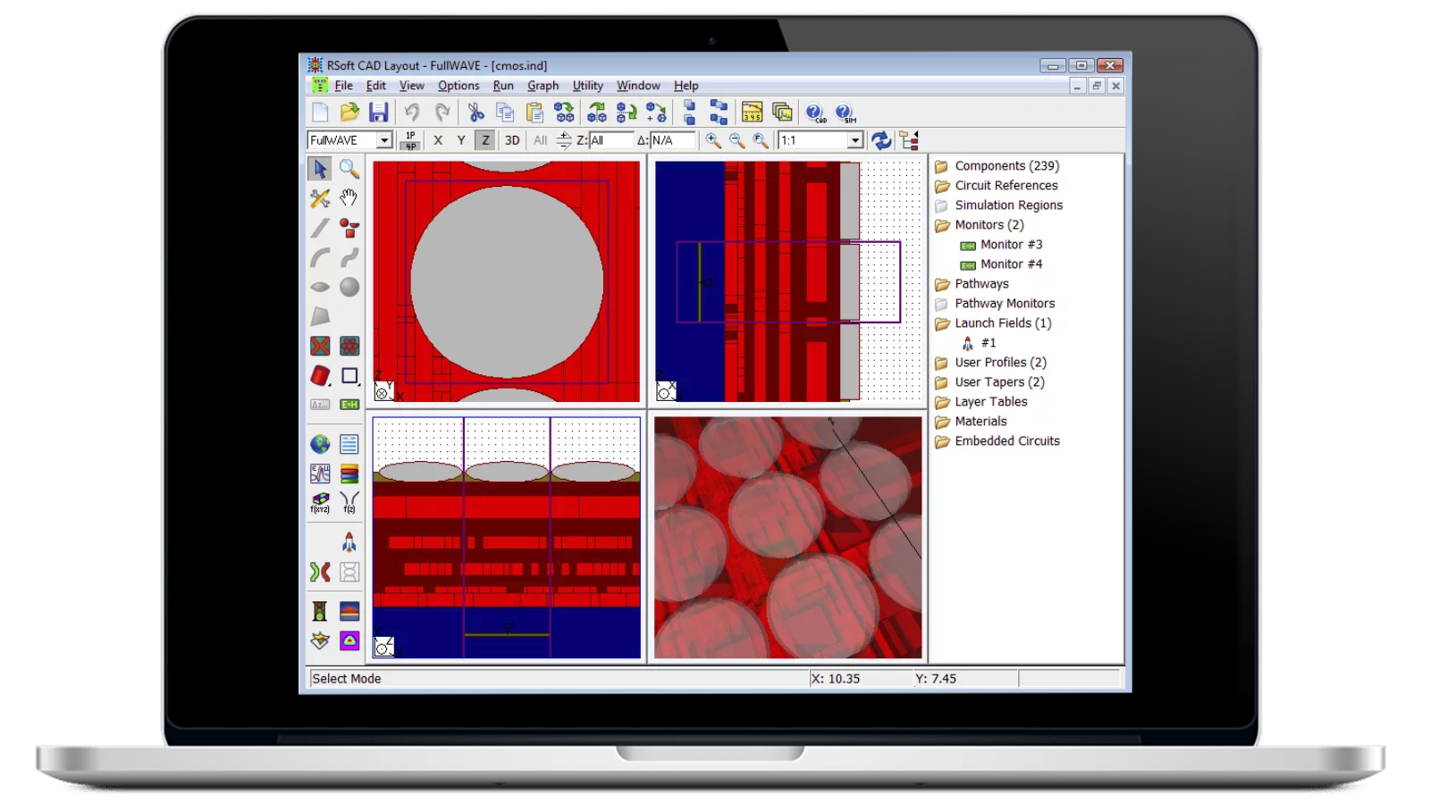
Why Use RSoft CAD Environment
One environment for photonic device design and optimization.
Designing photonic devices often requires multiple simulation methods, material models, and optimization approaches. The RSoft CAD Environment provides a common platform for creating device geometries, managing materials, configuring simulations, and transferring designs between photonic solvers.
Use RSoft CAD Environment for
- Creating 2D and 3D photonic device geometries
- Defining materials, refractive indices, and structural parameters
- Preparing models for multiple RSoft simulation methods
- Reusing a common device structure across different solvers
- Setting up parameter scans and design optimization studiesCalculating steady-state and dynamic laser behavior
- Importing and exporting layout data for photonic design workflows
- Managing simulation inputs, monitors, results, and post-processing

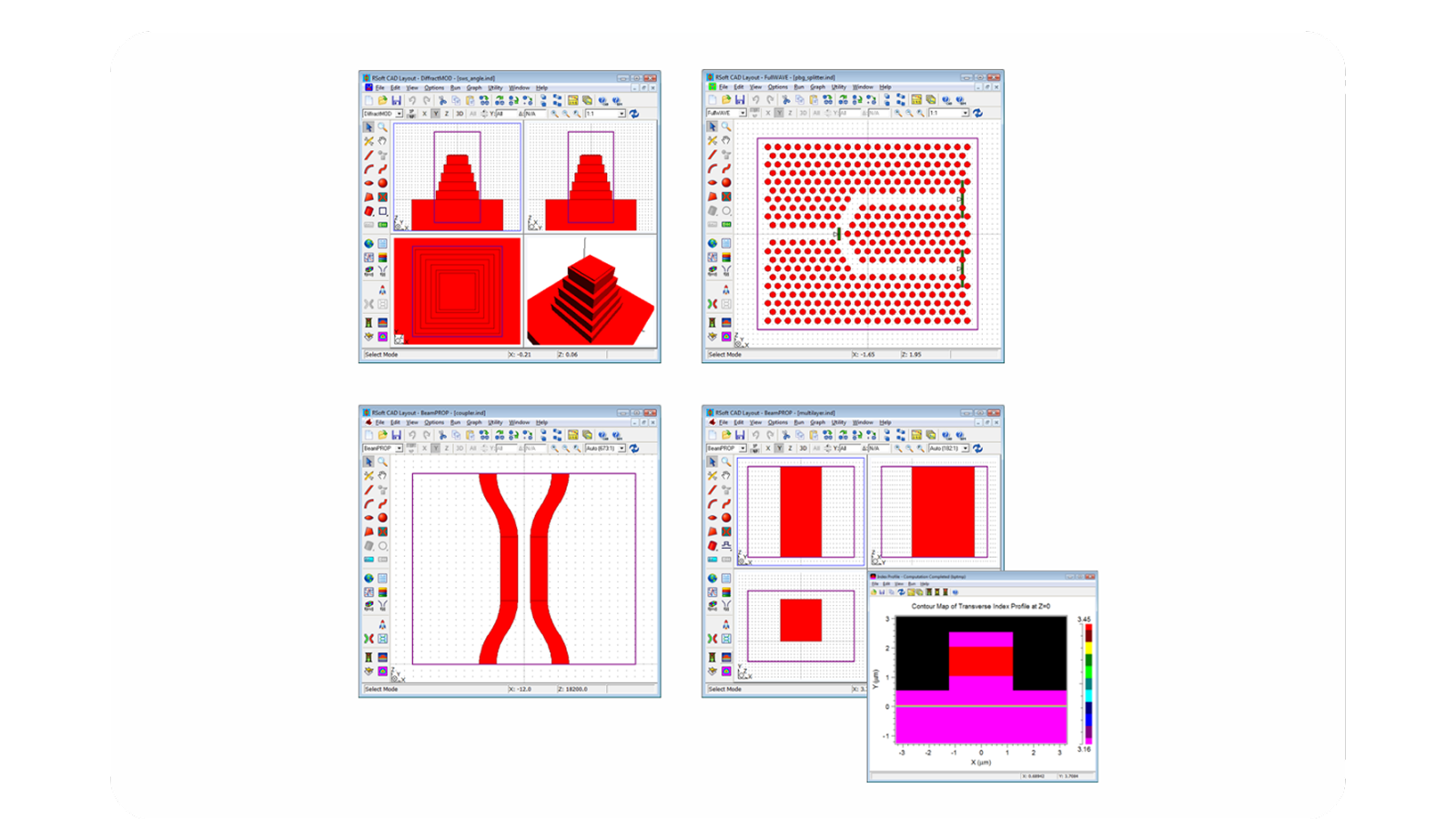
 Common Photonic Design EnvironmentCreate device geometries, assign materials, define simulation parameters, and manage results in one environment used across RSoft passive-device tools.
 Parametric and Object-Oriented ModelingBuild reusable photonic structures and vary dimensions, materials, and other design parameters without recreating the complete model.
 Multi-Solver Design ReusePrepare a device once and analyze it with the RSoft simulation method suited to each stage of development.
 Automated Design ExplorationConfigure parameter scans, scripted studies, and optimization workflows to evaluate design alternatives systematically.
Key Outcomes

Reuse device definitions instead of rebuilding geometry when changing simulation methods.

Evaluate variations in geometry, materials, or operating conditions from a common design environment.

Keep device definitions and simulation inputs organized as designs move between RSoft tools.

Prepare photonic structures and model data for subsequent optimization, compact-model, PIC, or optical-system activities.
Extend Device Design into PIC Development
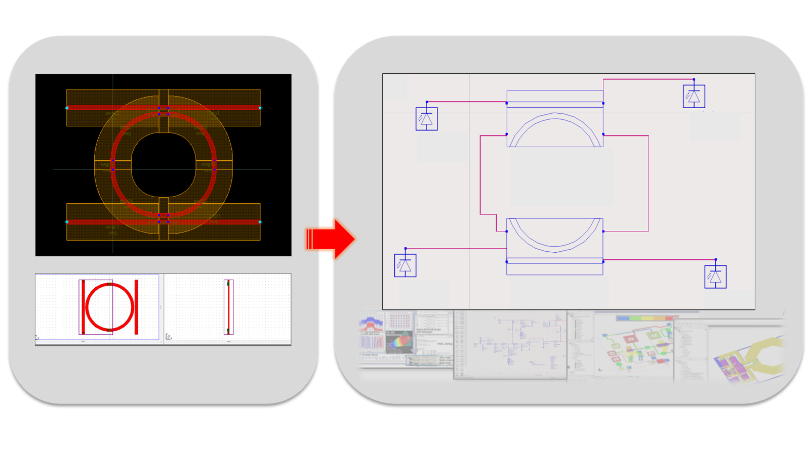
The RSoft CAD Environment serves as the foundation for photonic device workflows that can extend beyond component simulation. Optimized device designs can be used to generate compact models and custom PDK elements for use within ADS Photonic Designer, helping connect device-level analysis with photonic integrated circuit design and verification.

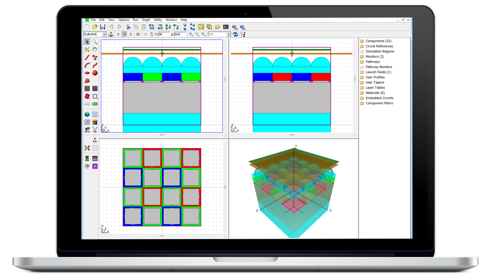
RSoft FullWAVE FDTD
Use the RSoft FullWAVE FDTD simulation tool to study how light propagates in photonic structures, circuits, and nanophotonic devices.
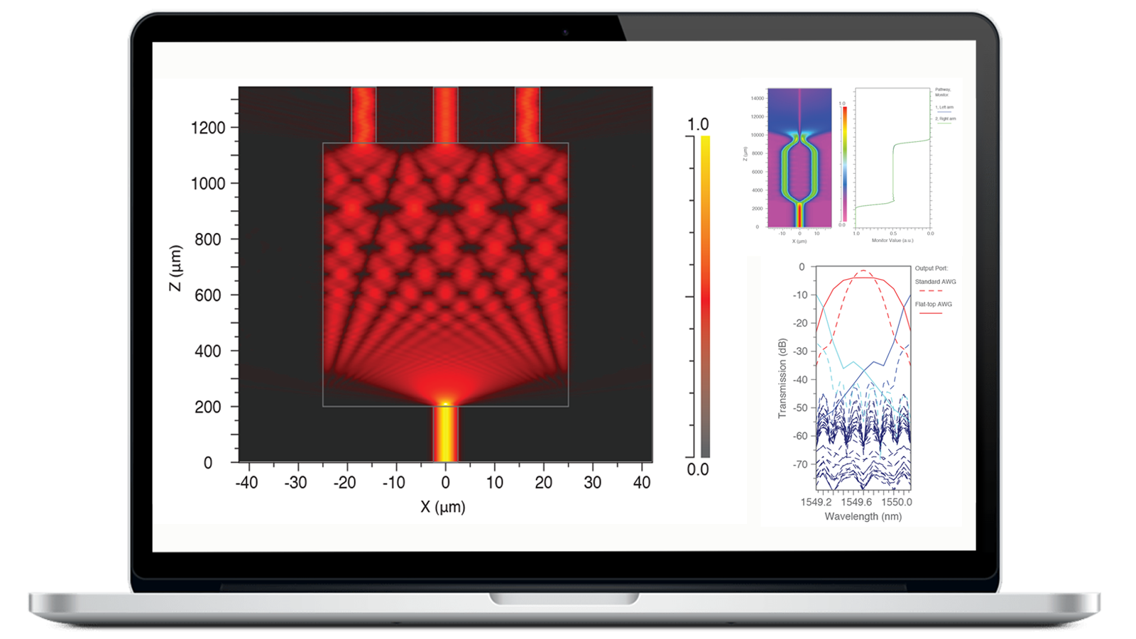
RSoft BeamPROP BPM
Use industry-leading RSoft BeamPROP BPM design software to rapidly and accurately design and simulate integrated and fiber-optic waveguide devices and circuits.
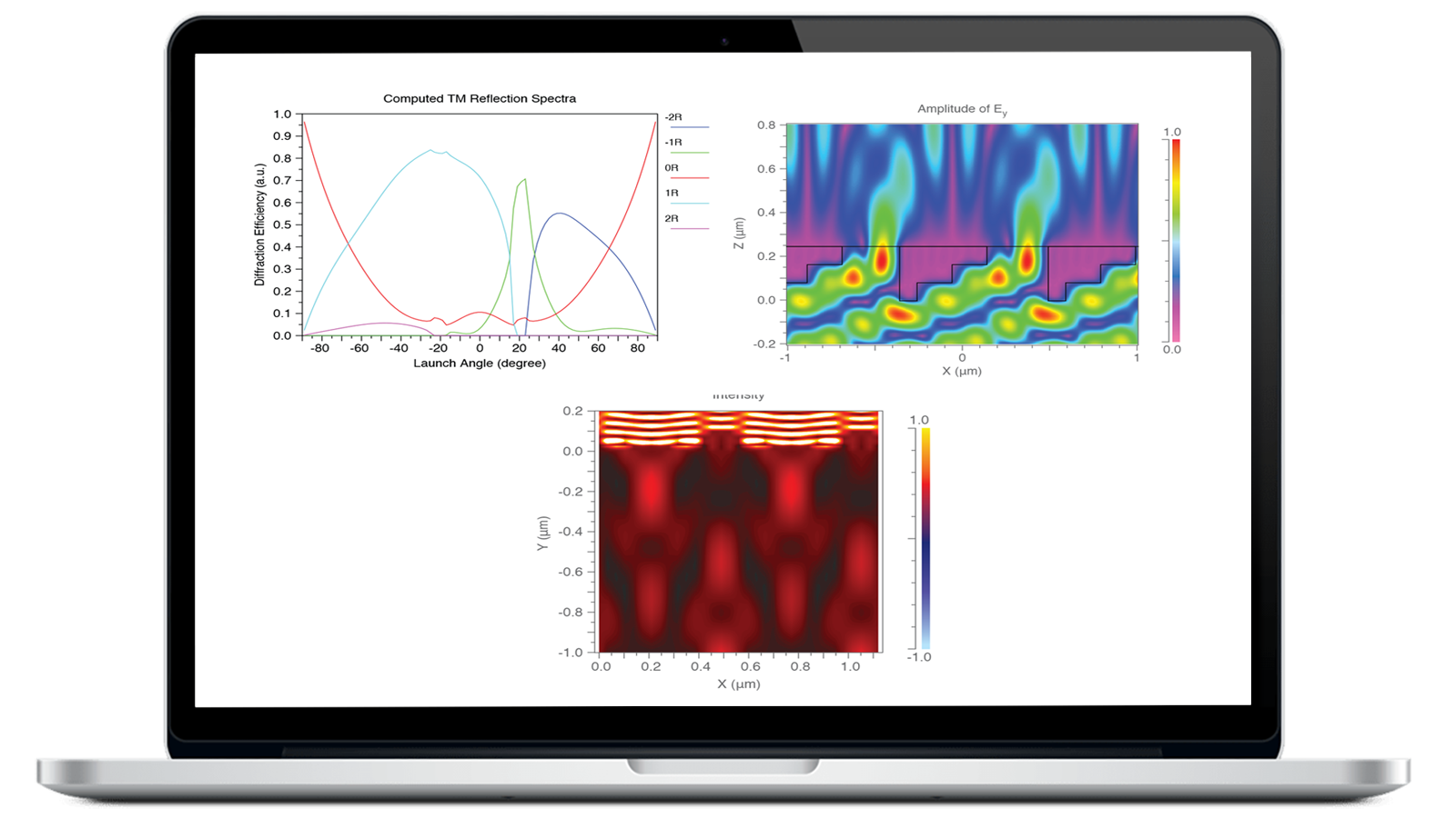
RSoft DiffractMOD RCWA
Use DiffractMOD RCWA design tool for diffractive optical structures, subwavelength periodic structures, photonic bandgap crystals, and more.
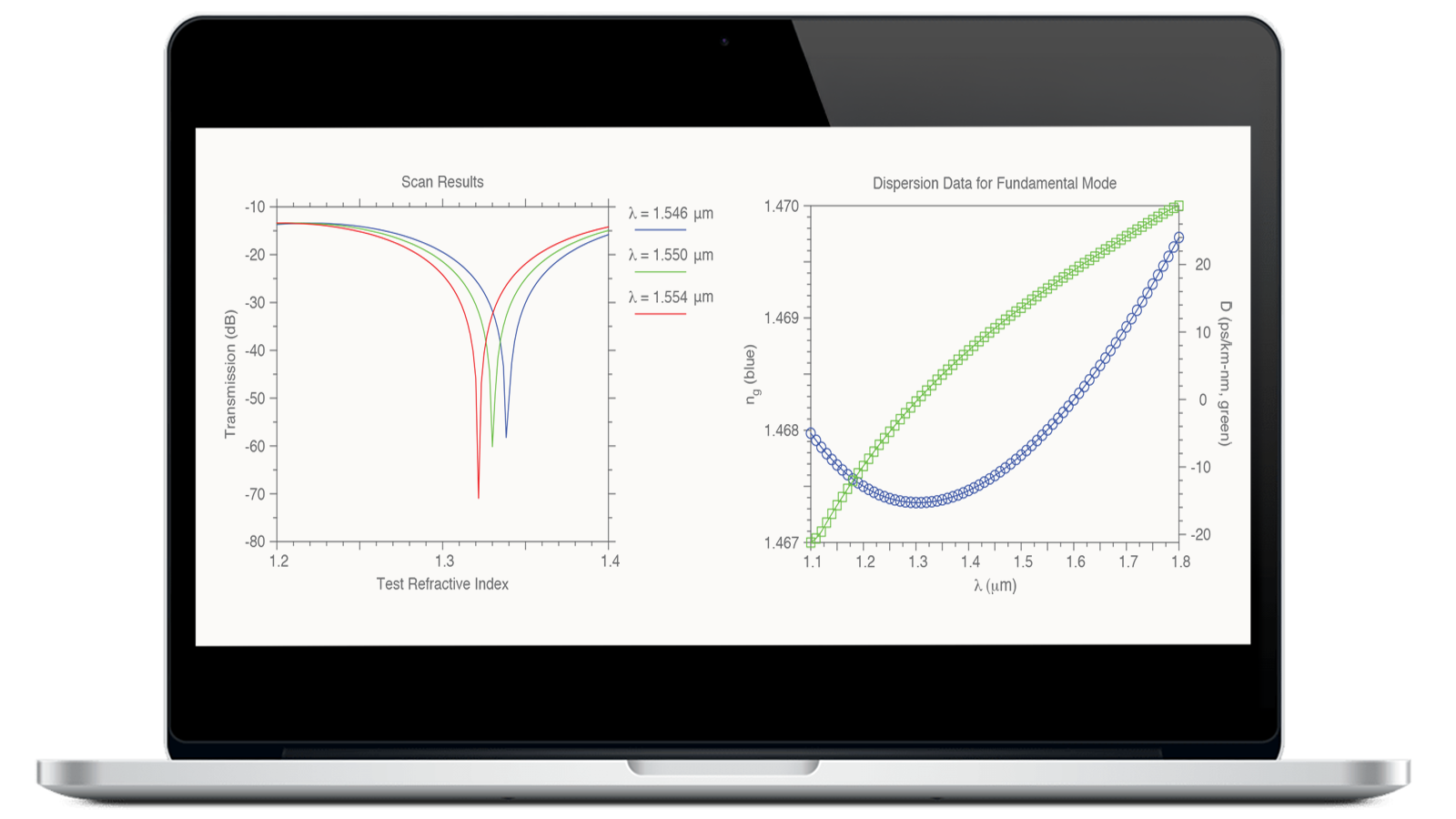
RSoft MOST
Use RSoft MOST or Multi-Variable Optimization and Scanning Tool to automate definition, calculation, and analysis of photonic device optimizations and scans.
Resources to Get You Started
应用文章
Patterned Surfaces using Data Files and Adding Coating Layers

应用文章
Design a Chiral Hologram using Metasurface
应用文章
Design of Gratings for Depth Sensing
白皮书
Choosing the Right Photonic Device Design Software
白皮书
Efficient and Accurate BPM Simulation of a Polarization
散页
What's New in RSoft Photonic Device Tools
Have Questions? We've Got Answers
A common design environment allows engineers to use multiple simulation methods and optimization tools without recreating device geometries or manually transferring designs between applications.
Yes. The RSoft platform supports multiple photonic simulation approaches, allowing engineers to evaluate device behavior using methods appropriate for different structures and applications.
You can specify each parameter of a component (for example, position coordinates, width, index) by an arithmetic expression involving user-defined variables, rather than simply being a constant number. This allows you to modify an entire design by using formulas to define each component's angle. You can also modify the entire circuit simply by changing the value of a single variable without having to edit multiple parts of the structure.
RSoft device designs can be used in workflows that generate compact models and custom PDK components for design activities in ADS Photonic Designer.
RSoft supports passive and active photonic devices including waveguides, gratings, photonic crystals, lasers, VCSELs, sensors, and other optical components.
RSoft provides a common design environment that supports multiple simulation methods, optimization tools, and connected workflows for photonic device development. It can also participate in broader design flows that connect device simulation with photonic integrated circuit design and verification.