


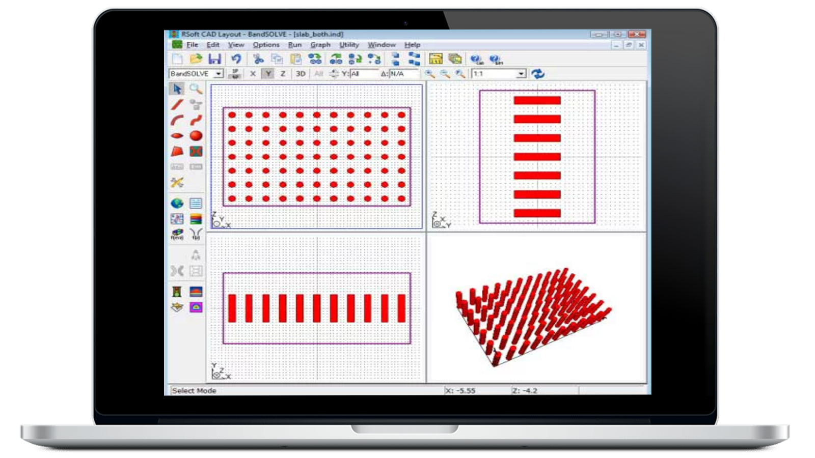
Why Use RSoft BandSOLVE PWE
Optimize the band structure of photonic crystal geometries.
Automate and simplify modeling and calculation of photonic band structures for all photonic crystal devices with RSoft BandSOLVE. BandSOLVE’s simulation engine employs a plane wave expansion (PWE) design tool to perform band computations. It also provides a graphical display of electromagnetic fields and other quantities for further analysis.
With a built-in array layout utility and layout hierarchy, your team can conveniently create standard and custom photonic band gap (PBG) structures. BandSOLVE also optimizes the band structure of new photonic crystal geometries before fabricating a device, allowing you to determine the performance of existing components.
Use RSoft BandSOLVE PWE for
- Calculating photonic crystal band structures
- Identifying photonic band gaps in periodic optical materials
- Designing photonic crystal waveguides and fibers
- Evaluating defect modes in photonic crystal structures
- Analyzing Bloch modes and light propagation in periodic structures
- Comparing photonic crystal geometries before fabrication
- Studying resonant cavities and other photonic crystal components

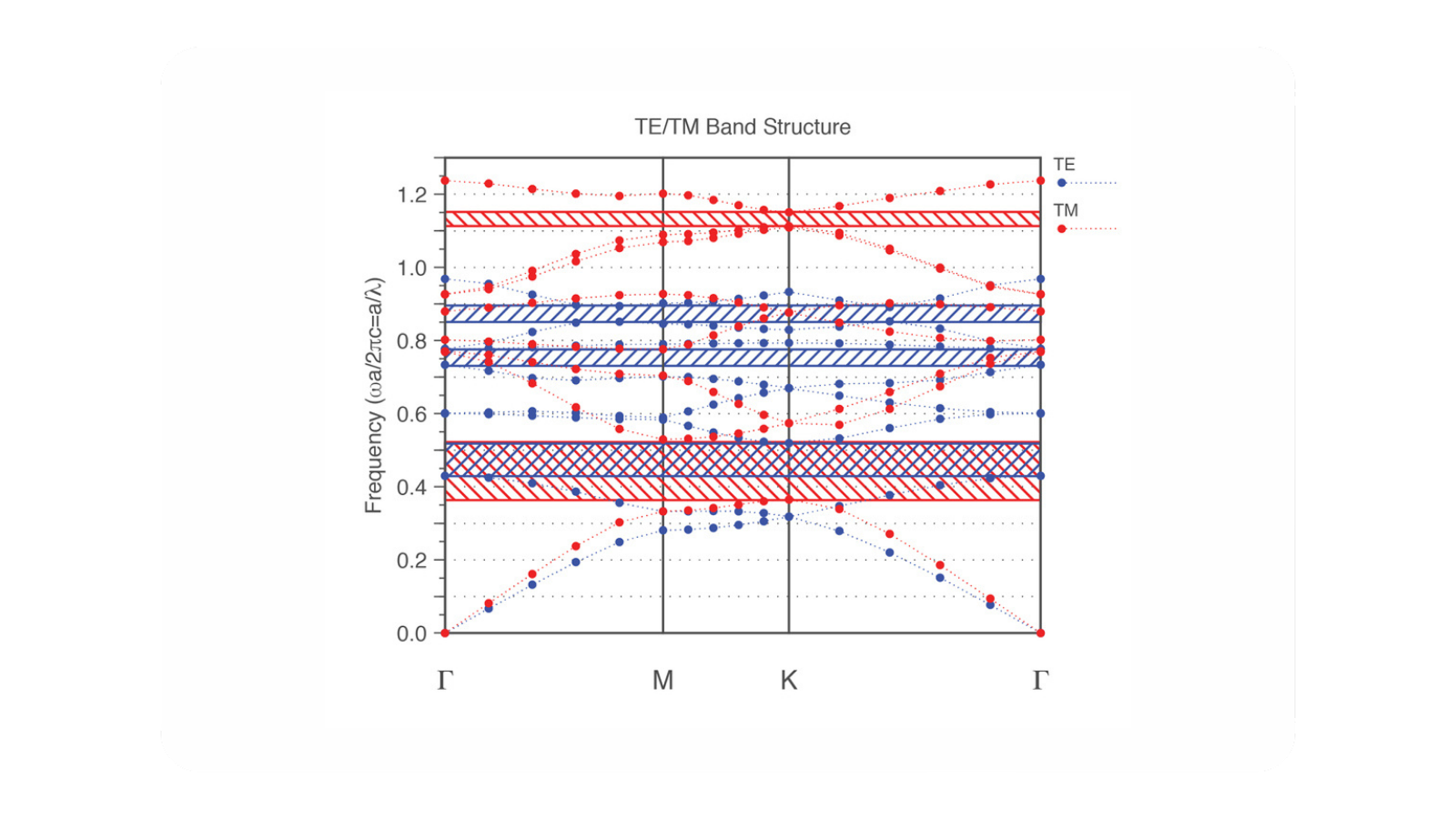
 Plane-Wave Expansion AnalysisCalculate photonic band structures and determine allowed and forbidden optical modes in periodic structures.
 1D, 2D, and 3D Photonic Crystal ModelingAnalyze periodic optical materials, photonic crystal slabs, fibers, waveguides, and three-dimensional structures.
 Mode and Field VisualizationExamine Bloch modes, defect modes, electromagnetic fields, and other characteristics of photonic crystal structures.
Key Outcomes

Determine frequency ranges in which light propagation is allowed or inhibited before fabricating the structure.

Examine Bloch modes, defect modes, and field distributions to understand how structural changes affect light propagation.

Evaluate alternative lattice, material, and defect configurations within a consistent simulation workflow.

Use band-structure results to select promising designs for more detailed electromagnetic analysis.
RSoft FullWAVE FDTD
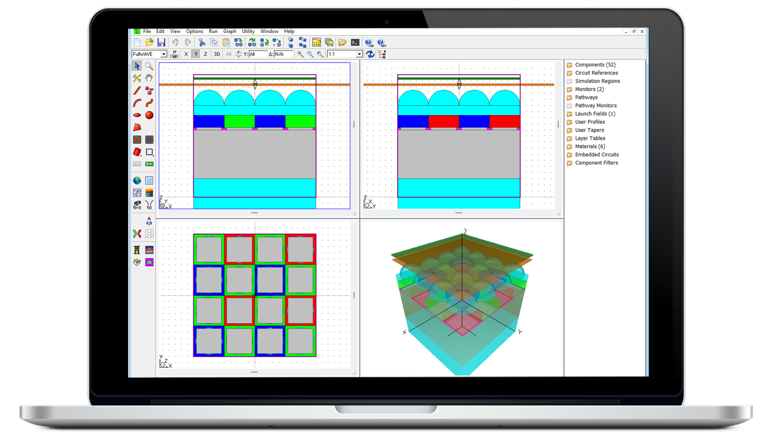
Use the RSoft FullWAVE FDTD simulation tool to study how light propagates in photonic structures, circuits, and nanophotonic devices.
RSoft FemSIM FEM
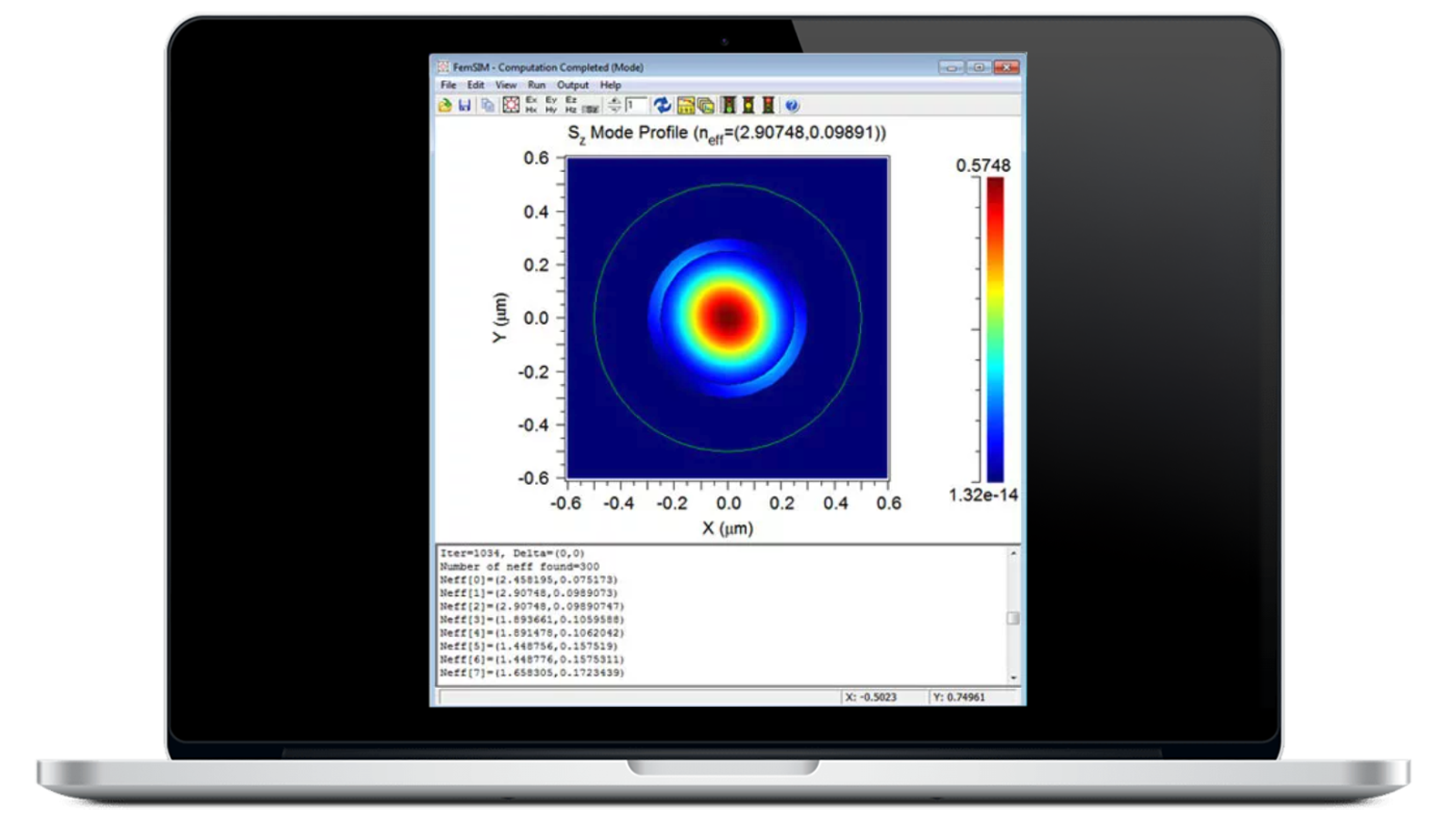
Use RSoft FemSIM FEM design tool to calculate any number of transverse or cavity modes of an arbitrary structure on a non-uniform mesh.
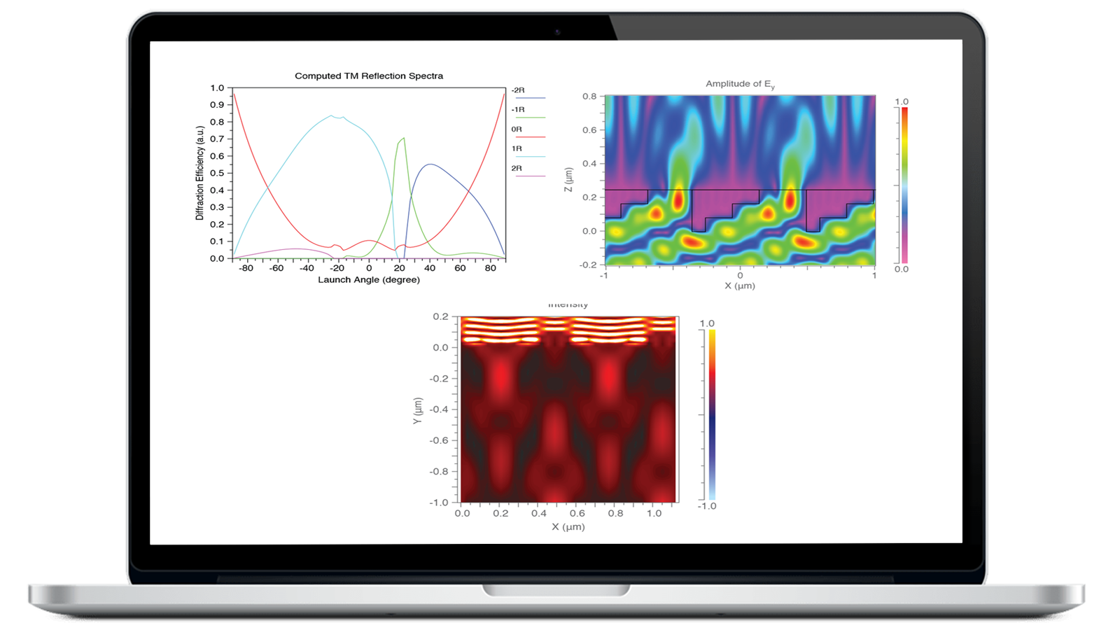
RSoft DiffractMOD RCWA
Use DiffractMOD RCWA design tool for diffractive optical structures, subwavelength periodic structures, photonic bandgap crystals, and more.
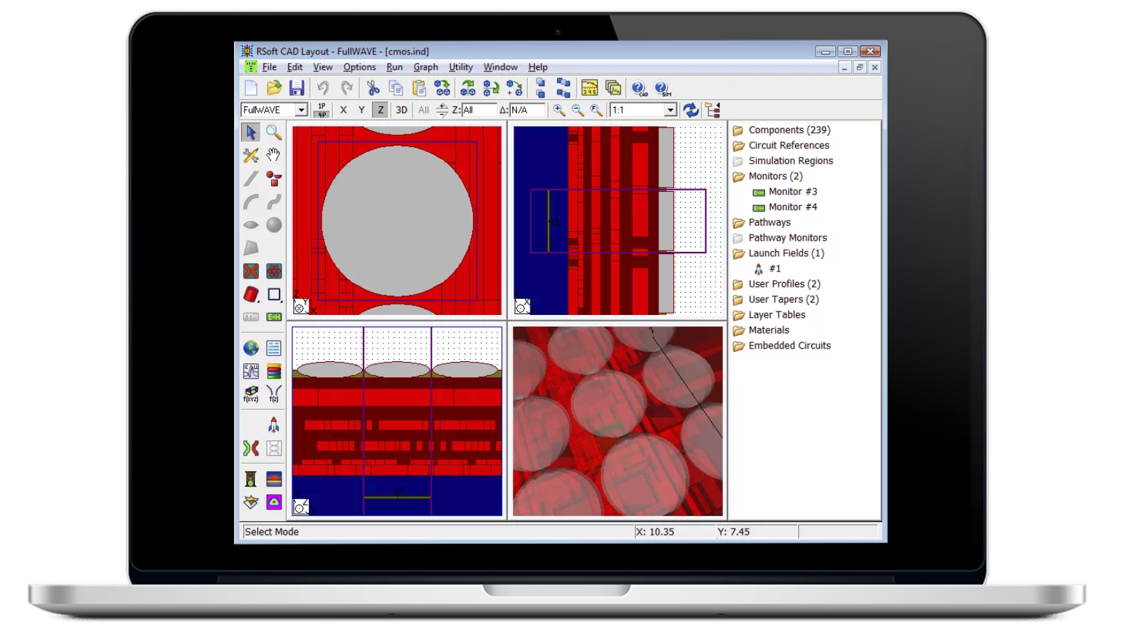
RSoft CAD Environment
The RSoft CAD Environment is the core program of the RSoft photonic device tools. Design waveguide devices, optical circuits, and other photonic devices.
Resources to Get You Started
Learn how band diagrams are used to analyze photonic crystal structures and identify photonic band gaps before fabrication.


Have Questions? We've Got Answers
The plane wave expansion (PWE) method is a frequency-domain simulation technique used to calculate the band structure of periodic optical materials and photonic crystals. By solving for the allowed and forbidden optical modes within a structure, PWE helps engineers understand how light propagates through photonic crystal devices and identify photonic band gaps.
A photonic band gap is a range of optical frequencies that cannot propagate through a periodic photonic crystal structure. Similar to the electronic band gap in semiconductors, photonic band gaps allow engineers to control and manipulate light for applications such as waveguides, filters, resonators, and integrated photonic devices.
PWE is typically used to analyze photonic band structures and identify photonic band gaps in periodic optical materials. It is often the preferred approach when studying the fundamental properties of photonic crystal structures.
FDTD simulation is generally used when engineers need to analyze the time-domain behavior of a device, study complex material effects, or evaluate optical performance beyond periodic band structure analysis. Many photonic crystal design workflows use both techniques at different stages of development.
BandSOLVE can be used to analyze a wide range of periodic photonic crystal structures, including one-dimensional (1D), two-dimensional (2D), and three-dimensional (3D) photonic crystal devices. Examples include photonic crystal waveguides, resonant cavities, photonic crystal fibers, and other periodic optical structures.
Yes. BandSOLVE includes capabilities for analyzing Bloch modes, defect modes, and other characteristics of photonic crystal structures. These capabilities help engineers evaluate how design modifications affect light propagation and device performance.
BandSOLVE is fully integrated within the RSoft CAD Environment, enabling a common design workflow across multiple photonic device simulation tools. Engineers can create and modify structures in the CAD environment, perform photonic band structure analysis with BandSOLVE, and leverage additional simulation methods available elsewhere in the RSoft tool suite as needed.